I. INTRODUCTION
In recent years millimeter-wave (mm-wave) applications have attracted increasing attention for a wide variety of reasons. Growing demands for higher data transfer rates in telecommunications, higher resolution in radio imaging systems, and more precise target detection in radars can ultimately be met by increasing the absolute frequency bandwidth. This is, however, not straightforward at ultra high frequency (UHF) and super high frequency (SHF) ranges since they are densely occupied and their percentage bandwidth is considerably high. Another industrial motivation for moving toward higher frequencies is a higher integration level – a consequence of size reduction. This trend has been accelerated by exceptionally rapid progress in semiconductor technologies, which has led to the development of transistors with transition- and maximum oscillation frequencies (f T, f max) in the range of hundred's of GHz [Reference Heinemann2]. Mm-wave devices with operating frequencies in the range of 100 to 200 GHz and even beyond have already been reported for industrial, scientific, and medical applications [Reference Sarmah3–Reference Yanfei6]. Despite all these benefits that have encouraged circuit designers to develop mm-wave integrated circuits (ICs), some challenging issues become more noticeable at higher frequencies: for example, higher resistivity due to skin- and proximity effects that increase the loss in passive structures, and exponentially growing free space path loss, which limits the communication range of wireless systems. Furthermore, there are numerous complexities in connection with experimental verification and characterization of mm-wave circuits, since the parasitics are no longer negligible and the characteristics of the material may not be known at such frequencies.
From a system point of view, antenna integration has remained a challenging issue. Antenna size, the feeding network of the antenna, and isolation from other components are three main concerns in this context. Antenna size and isolation are less critical for off-chip antennas, for instance, realized on a printed circuit board (PCB). In this case, the antenna is usually interconnected with the IC by bond wires or by a flip-chip technique. Regardless of the type of interconnection, a very high transition frequency between IC and PCB must be handled, and hence expensive PCBs with particular radio frequency (RF) characteristics are necessary. A well-known alternative approach to avoiding RF interfaces and lowering the fabrication costs is to integrate antennas with all other building blocks on a single chip and create a system-on-chip (SoC) [Reference Cheema and Shamim7]. Although this technique benefits from the highest level of integration, it suffers from a couple of fundamental problems; an extremely limited antenna size and the lossy nature of the silicon substrate result in a basic trade-off between antenna performance and level of integration. Reducing the thickness of the lossy substrate [Reference Baek8] and employing additional discrete elements such as a superstrate [Reference May9] or a lens [Reference Babakhani10] have been proposed to improve performance of SoCs. These techniques, however, are in a fundamental conflict with the concept of miniaturization, and usually they are not compatible with mass production.
A different integration solution that has become popular with the latest advances in assembly and packaging technologies is a fully integrated system-in-package (SiP) [Reference Liu11, Reference Zhang and Liu12]. The basic concept behind this approach is to separate IC and antenna from each other while integrating them in a single package. In fact, a SiP is an in-between solution which profits from a high integration level and a relatively high antenna performance. Various SiPs with different fabrication methods have been published. One of the novel approaches that have enabled low-cost highly integrated SiPs is the embedded wafer level ball grid array (eWLB) process, introduced in [Reference Brunnbauer13–Reference Boeck16]. Fully integrated 77-GHz SiPs designed for automotive radar applications and built using eWLB technology have already been reported in [Reference Fischer17–Reference Hasch19]. In this work, we present a 160-GHz SiGe-based transmitter (TX) and receiver (RX) interconnected with highly directional tilted square antenna arrays and integrated in eWLB packages. The TX- and RX-chips were separately characterized by a set of on-wafer measurements, and the functionality of the SiP was successfully demonstrated in several practical experiments.
II. SiP CONCEPT
In the eWLB technology a mold wafer is manufactured with embedded ICs as described in [Reference Brunnbauer13–Reference Boeck16]. Figure 1 depicts a simplified cross-sectional view of an eWLB package mounted on a PCB. The area enclosed by the sidewalls of the IC and the extended package area surrounding the IC are known as the fan-in and the fan-out area, respectively. On a redistribution layer (RDL) passive structures such as transmission lines (T-lines), inductors, and antennas can be designed in the fan-out area and interconnected to the IC.

Fig. 1. Simplified cross-sectional view of an eWLB package mounted on a PCB with desired direction of radiation along θ = 0°.
A comparison of different studies conducted in [Reference Wojnowski15] and [Reference Hamidipour20] proves a considerably smaller attenuation constant for the T-lines which were realized on the RDL compared with their on-chip counterparts. Although the attenuation constant reported for a 70 Ω differential T-line in eWLB package is less than 0.5 dB/mm at 77 GHz [Reference Wojnowski15], it exceeds 1.5 dB/mm for a 70 Ω on-chip differential T-line [Reference Hamidipour20]. The electrical connections between the RDL and PCB are done by a set of solder-balls. In this case, there was no need for high-frequency signal transition between the IC and the PCB. Therefore the solder-balls were only used for transition of local oscillator (LO) and intermediate frequency (IF) between the IC and the PCB. As stated in [Reference Boeck16], the mold compound has a relatively high thermal resistance compared with metal or silicon. Therefore thermal energy of the IC flows mainly via the solder-balls rather than being dissipated in the mold compound or being radiated to the air. A temperature analysis presented in [Reference Boeck16] reveals that the solder-balls, which are located in the fan-out area have a minor impact on the heat transfer to the PCB. In other words, the heat dissipation is mainly done by the so-called thermo-balls, which directly interconnect the IC to the PCB. From an electrical point of view the thermo-balls are typically terminated to the ground connection of the IC and are distributed in areas which are not critical for RF functionality [Reference Wojnowski15, Reference Boeck16].
Regardless of the number of metal layers, on-chip passive structures are generally realized within a relatively thin (typically <20 µm) insulating layer (e.g. SiO2) which is stacked on a relatively thick (typically >300 µm) semiconductor substrate (e.g. Si) with a comparatively high dielectric constant (typically εr > 11) [Reference Cheema and Shamim7]. On the other hand, the typical distance between the RDL and the PCB after soldering is in the range of 180 µm [Reference Fischer18]. Considering the fact that this space is usually not filled with any dielectric layer except for two thin (5–10 µm) organic layers which are supposed to isolate the IC and the RDL [Reference Boeck16], the impact of the PCB was neglected in this work.
III. IC DESIGN
A) Transmitter
The chip set was realized using Infineon's high-speed SiGe:C production process B7HF200. As described in [Reference Hamidipour21], this technology offers HBTs with f T and f max of about 170 and 250 GHz, respectively. Designing a 160 GHz transceiver (TRX) with such transistors is a challenging task. Although the operating frequency approaches f T and f max, the power loss of the building blocks increases significantly. Moreover, a fundamental oscillator and mixer may no longer sustain at such frequencies. With a harmonic approach, such difficulties can be ameliorated because the building blocks are usually designed at a fraction of the final frequency. The main drawback of this technique is a comparatively larger chip is required for a higher number of building blocks and lower output power. In a SiP, however, this problem is less critical than in a SoC because the antenna is already located off the chip. Therefore, a harmonic approach with a fundamental LO frequency of around 80 GHz and a second harmonic of 160 GHz was chosen in this work. As shown in Fig. 2(a), the 80-GHz fundamental LO signal (LOM) is generated by a frequency multiplier chain with a total multiplication factor of 18 (×18), including a frequency doubler (×2) and two frequency triplers (×3) [Reference Fischer22]. Figure 2(b) presents a microphotograph of a multiplier test chip which was fabricated for characterization of the (×18) multiplier. In addition, a microphotograph of the 160-GHz TX-chip realized on a 2006 × 1865 µm2 silicon die and embedded in an eWLB package is presented in Fig. 2(c). The ×18 multiplier is preceded by an active balun (AB) and a variable gain amplifier (VGA). The AB allows a single-ended input signal (LOIN) from a commercial signal source to be used, and the VGA regenerates the LOIN, which can be reused in a daisy chain topology. The LOM is routed through a local oscillator buffer (LOB), a power amplifier (PA) with a measured gain of about 10 dB [Reference Hamidipour21], and a Gilbert-cell-based frequency doubler, which finally scales the frequency up to about 160 GHz (RFOUT). The differential LOM of the multiplier test chip shown in Fig. 2(b) was measured while the frequency of LOIN was swept from 3.6 to 5 GHz. As plotted in Fig. 3(a), the measurements show a saturated output power with a center frequency of about 80 GHz for an arbitrary input power level in the range of −20 to 5 dBm. In addition, a phase noise (PN) measurement was performed using an SME06 signal source and an FS-Z90 harmonic mixer from Rohde&Schwarz, and an E5052A signal source analyzer from Agilent. As indicated in Fig. 3(b) PNs below −90 dBc/Hz were achieved at a frequency offset of 100 KHz. To evaluate the functionality of the last three stages of the TX circuit, an additional test chip containing the LOB, the PA, and ×2 multiplier was fabricated. At an input power level of 0 dBm, the output power of this test chip was measured whereas the input frequency was swept from 65 to 90 GHz. Figure 4 presents the measurement results and a microphotograph of the fabricated doubler test chip. An acceptable frequency centered at around 160 GHz with a maximum output power of nearly 0 dBm was obtained.
Fig. 2. Block diagram of the TX (a), Microphotograph of the multiplier test chip (b), and microphotograph of the TX-chip realized on a 2006 × 1865 µm2 silicon die embedded in an eWLB package (c).
Fig. 3. On-wafer measured differential output power (a) and phase noise (b) of the multiplier test chip. A maximum output of about −2 dBm was achieved at 80 GHz.
Fig. 4. On-wafer measured differential output power of ×2 preceded by the PA and the LOB (a) and microphotograph of the doubler test chip fabricated for experimental evaluation of the ×2 multiplier (b). A maximum output of around 0 dBm was achieved at 160 GHz.
B) Receiver
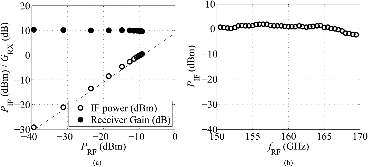
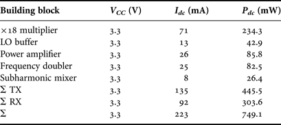
The RX-chip incorporates a similar LO distribution scheme integrated with a Gilbert-cell-based subharmonic mixer (SHM) on an identical chip area of 2006 × 1865 µm2. The simulated output power from the LOB delivered to the SHM was in the range of 0 to 6 dBm over a 10-GHz frequency band from 75 to 85 GHz. For this LO power range, the SHM showed a simulated double-sideband noise figure below 20 dB with a minimum value of about 16.5 dB. Additional LO amplifiers were therefore unnecessary. Since the frequency of the RF input signal (RFIN) and the f T of the technology were of comparable magnitude, RF amplifiers were avoided. To assess the performance of the RX circuit experimentally, a discrete test chip including the LOB and the SHM was manufactured and measured. Figures 5(a) and 5(b) present a block diagram and a microphotograph of this test chip, respectively. In conjunction with a Rohde&Schwarz ZVT20 network analyzer, different frequency extender modules from Rohde&Schwarz and OML were employed to generate the LO and RF test signals. The frequency extenders were available at different waveguide frequency bands from 75 to 110 GHz (W-band) and from 110 to 170 GHz (D-band) with a maximum saturated output power of about +5 and −5 dBm, respectively. The differential IF output was converted to single-ended by a commercial 0-dB gain instrumentation amplifier with 100 k ga input impedance, and monitored by a Rohde&Schwarz FSQ spectrum analyzer. Figures 6(a) and 6(b) show the measured IF power (P IF) of the mixer test chip in Fig. 5(b) in terms of the RF power (P RF) and the RF frequency (f RF), respectively. Both measurements were performed at an LO power level (P LO) of about 0 dBm and a constant 4-MHz frequency shift between f LO and f RF. Considering a −5-dBm maximum saturated output power from the D-band frequency-extender and a nearly 4-dB insertion loss of the auxiliary WR-06 S-bend in conjunction with the Picoprobes from GGB (necessary for contact with the wafer) the P RF delivered to the SHM could not exceed −9 dBm. Although the conversion gain of the SHM was successfully measured in this experiment, the P RF was not sufficiently high to measure the 1-dB input compression point, which was around −4 dBm in the simulation. Table 1 summarizes the current drawn and power consumption of all the building blocks which were run on an identical 3.3 V supply voltage in both TX- and the RX-chips.
Fig. 5. Block-diagram (a) and microphotograph (b) of the mixer test-chip fabricated for experimental evaluation of the SHM.
Fig. 6. Measured P IF and G RX versus P RF at P LO = 0 dBm, f LO = 80.000 GHz, and f RF = 160.004 GHz (a). Measured P IF versus f RF at P LO = 0 dBm, P RF = −10 dBm, and an offset frequency of 4 MHz between LO and RF (b).
Table 1. Power consumption of the building blocks.
IV. ANTENNA DESIGN
To take maximum advantage of the space provided in the fan-out area, a compact differential antenna array was designed. As shown in Fig. 7, seven square loop elements are tilted and distributed in two rows along the y-axis to form a right-angled rhombic antenna array. Each rhombic element has a side length of nearly ≈λ g/4, where λ g indicates the guided wave-length in the fan-out area of the package at 160 GHz. The connections between the elements were accomplished by ≈λ g/2 lines oriented along the x-axis. Such an arrangement leads to an identical current distribution on the rhombic elements and consequently results in a maximum radiation broadside to the angle of the array as explained in [Reference Hamidipour23]. A full 3D simulation of the rhombic antenna array in conjunction with the IC, the interconnections, the solder-balls, and the PCB was carried out in CST microwave studio suite. The resulting radiation beam pattern at 160 GHz is plotted in Fig. 8 for Φ = 0° (H-plane) and Φ = 90° (E-plane). As the rhombic elements are distributed along the y-axis, a wider beam pattern is obtained in the H-plane compared to the E-plane. Such a relatively wide beam pattern is suitable for short-range radar applications, where various targets at different angles of view must be detected. A multi-section differential matching structure connects the antenna and the IC as indicated in Fig. 7. Additionally, the width of the rhombic elements and their interconnections were adjusted to obtain a stable impedance matching over a broad frequency band. Figure 9 presents the reflection coefficient S 11 of the antenna calculated at the reference plane shown in Fig. 7, and the antenna gain (G) versus frequency evaluated along θ = 0°. An impressive bandwidth of more than 20 GHz with a broadside gain of more than 5 dBi was achieved from 150 to 170 GHz.
Fig. 7. A microphotograph of the fabricated 160-GHz AiP integrated with the 160-GHz TX chip in a 6 × 6 mm2 eWLB package.
Fig. 8. Simulated radiation beam pattern of the rhombic antenna array versus θ in E-plane (Φ = 90°) and H-plane (Φ = 0°) (Φ = 0°) at 160 GHz.
Fig. 9. Plots of S 11 calculated at the reference plane shown in Fig. 7 and the antenna gain calculated at θ = 0° in terms of frequency.
V. THE RADAR APPLICATION
By soldering the fabricated TX and RX packages on separate low-cost PCBs, a single-channel quasi-monostatic FMCW radar frontend was constructed. To showcase the functionality of such a radar frontend in a range measurement application two discrete experiments were performed in an anechoic chamber with three corner reflectors as targets. In the first experiment, the targets were chosen to have different radar cross sections (RCSs) and were placed at different radial distances from the frontend. In the second experiment, however, identical targets were positioned at different angles of view but at the same distance from the frontend. Figures 10(a) and 10(b) illustrate the arrangement of the targets and the frontend in the two experimental setups, respectively. In both experiments, a commercial frequency synthesizer was used to generate LOIN with the required frequency ramp [Reference Ng1]. In addition, a digital baseband board with a field-programmable gate array (FPGA) [Reference Pfeffer24], a PC, and a power supply which supplied the frontend and the baseband board were employed. The FPGA was configured to control the digital-to-analog converters, the analog-to-digital converters, and the communication between the baseband board and the PC. As the second experiment was conducted in the azimuth plane, the radar frontend was rotated by 90°. Both experiments were performed with a 1-ms up-chirp frequency sweep from 157 to 160 GHz. The power spectra of the acquired IF signal of the two experiments are plotted in Fig. 11(a) and (b), respectively. The targets were clearly detected with an adequate signal-to-noise ratio. Although the targets were located at the same radial distances from the frontend in the second experiment, the amplitudes of their acquired IF spectrums are noticeably different. This is mainly due to different antenna gains at θ = −40° and θ = 40°. Nevertheless, the results demonstrate a relatively wide angle of coverage which is appropriate for short-range radar applications.
Fig. 10. FMCW measurement setups with the 160-GHz radar frontend and three corner reflectors at different radial distances (a) and at different angles of view (b). A 1 euro coin is shown for size comparison.
Fig. 11. IF spectrum of a 1-ms up-chirp FMCW experiment with a frequency sweep from 157 to 160 GHz. In the first experiment, targets were placed at different radial distances (a), whereas in the second experiment the targets were positioned at the same distance but different angles.
VI. THE IMAGING APPLICATION
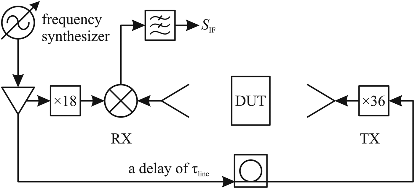
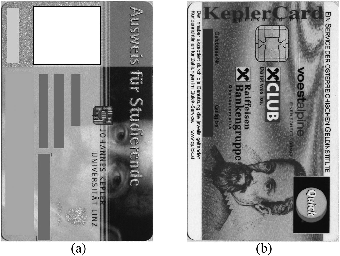
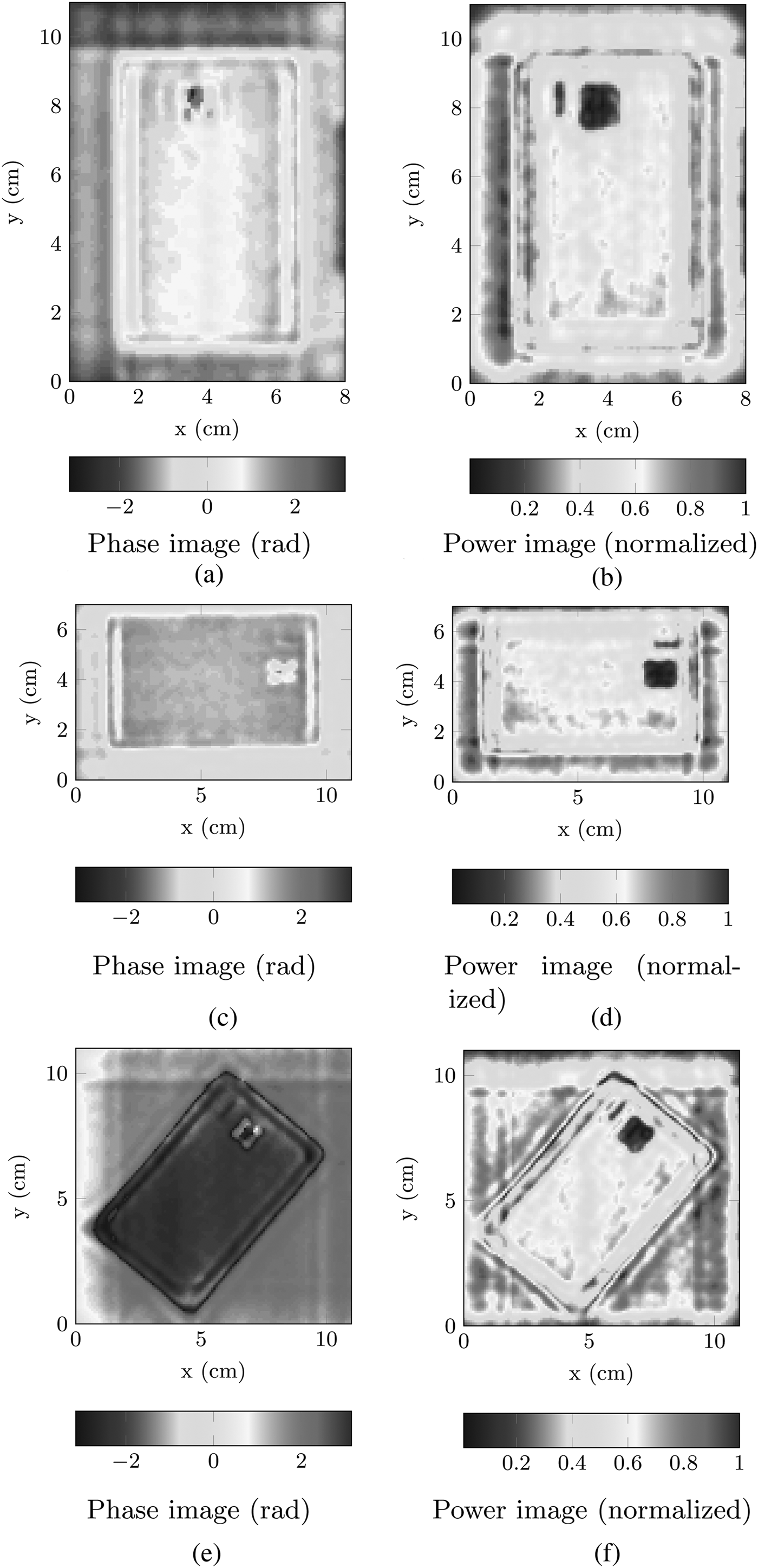
A mm-wave system with a typical bandwidth of a few GHz is a potential candidate for radio imaging applications, where a wide bandwidth allows a depth focus on the image. To investigate the performance of our proposed SiP in an imaging application, a forward-scatter FMCW radar was constructed with an 8 GHz frequency ramp from 157 to 165 GHz [Reference Feger25, Reference Feger26]. Figure 12 shows a block diagram of this measurement setup including the 160-GHz TX and RX, the frequency synthesizer for ramp generation (similar to that in section I), LO distribution lines, and an arbitrary DUT. As shown in Fig. 12, the extra line length between the TX and the RX causes a delay of τ line. Since the arrangement of the setup was not changed during the experiment, the value of τ line was easily measured and calibrated in a preliminary experiment. Figure 13 presents a university ID card with RFID functionality, which was used as the DUT in this experiment. To capture a full-scale image, the ID-card was moved in steps along in a rectangular 0.95 mm grid by a high-precision positioning stage. The captured data were sampled by an external analog-to-digital converter and analyzed on a PC, where a back projection algorithm was used to generate the mm-wave images. With the complex data of this experiment either a phase- or a power-image could be calculated.
Fig. 12. Block diagram of the forward-scatter FMCW radar setup including an LO frequency synthesizer, an arbitrary DUT, the 160-GHz TX and RX, and a 4.5-GHz LO distribution line with a delay of τ line.
Fig. 13. Front (a) and back (b) of the university ID card with RFID functionality used as DUT in the imaging experiment.
Although the RFID components of the ID card are invisible to the naked eye, they are readily visible in the phase and power images obtained in our experiment. The ID card was scanned in three different orientations to demonstrate effects of polarization. In Figs 14(a) and 14(b), the ID card was scanned in an upright position. In the phase image, the parts of the integrated RFID antenna that are positioned alongside the longer edge of the card can be clearly seen. Here, the corresponding parts of the RFID antenna are parallel to the E-field vectors. The power image shows the main chip of the card (visible to the naked eye) and a second chip next to it. Figures 14(c) and 14(d) present the scanned images of the ID card rotated by 90° which reveals the other parts of the antenna alongside the short edge of the DUT. The third scan was executed with the ID card positioned at an angle of 45°, which can be seen in Figs 14(e) and 14(f). The phase image shows the whole antenna, but with less contrast than the previous images.
Fig. 14. Phase and power images of the ID card shown in Fig. 13 for an up-right position (a, b), a 90° rotated position (c, d), and a 45° rotated position (e, f). The power images were normalized to the maximum value and plotted in a linear scale.
VII. CONCLUSION
Recent progresses in packaging technologies have led to the development of miniaturized AiPs with superior performance and reliable connections to the ICs. As a result, design and implementation of highly integrated SiPs for mm-wave applications have attracted growing interest. One of the well-known fabrication processes that has proven promising for mm-wave packaging is the eWLB technology. In this work, we took advantage of attractive features of this technology to design a highly integrated 160-GHz SiP and demonstrate it in different practical applications. In the first step, separate TX- and RX-chips were designed in a commercial SiGe:C process offering HBTs with f T and f max of about 170 and 250 GHz, respectively. The fabricated 2006 × 1865 µm2 ICs were embedded in 6 × 6 mm2 eWLB packages and interconnected with highly directional rhombic antenna arrays. By soldering the fabricated packages on separate PCBs, a quasi-monostatic FMCW radar frontend was built and successfully deployed in a 1-ms 3-GHz up-chirp FMCW range detection measurement with three corner reflectors as targets. In addition, a forward-scatter FMCW radar experiment with 8-GHz bandwidth and an arbitrary DUT was conducted. The experiments clearly show the suitability of the proposed SiP for various mm-wave applications.
ACKNOWLEDGEMENTS
This work has been (partially) supported by the Austrian COMET-K2 programme of the Linz Center of Mechatronics (LCM), and was funded by the Austrian federal government and the federal state of Upper Austria.
 Abouzar Hamidipour received the B.Sc. degree from the Iran University of Science and Technology, Tehran, Iran in 2004, and the M.Sc. degree from the Sahand University of Technology, Tabriz, Iran, in 2007, both in electrical engineering. He is currently with the Institute for Communications Engineering and RF-Systems at the Johannes Kepler University, Linz, Austria, where he is pursuing the Ph.D. degree in electrical engineering. His research interests include the design and implementation of highly integrated system-in-packages (SiPs) for millimeter-wave applications; antennas and propagation; and microwave photonics.
 Reinhard Feger was born in Kufstein, Austria, in 1980. He received the Dipl.-Ing. (M.Sc.) degree in mechatronics and Dr. techn. (Ph.D.) degree in mechatronics from Johannes Kepler University, Linz, Austria, in 2005 and 2010, respectively. In 2005, he joined the Institute for Communications and Information Engineering, Johannes Kepler University, as a Research Assistant. In 2007, he became a member of the Christian Doppler Laboratory for Integrated Radar Sensors, Johannes Kepler University. His research topics are radar signal processing, as well as radar system design for industrial and automotive radar sensors. Dr. Feger was recipient of the 2011 Microwave Prize and the 2011 German Microwave Conference Best Paper Award. In 2012, he received the Best Measurement Paper Prize at the European Conference on Antennas and Propagation.
Sebastian Poltschak was born in Linz, Austria, in 1988. He received the B.Sc. degree in Information Electronics from Johannes Kepler University, Linz, Austria, in 2012. He is currently working toward his master's degree in Information Electronics at the Institute for Communications Engineering and RF-Systems, Johannes Kepler University, Linz, Austria. His research topic is radar imaging.
 Andreas Stelzer was born in Haslach an der Mühl, Austria, in 1968. He received the Dipl.-Ing. degree in Electrical Engineering from the Technical University of Vienna, Vienna, Austria, in 1994, and the Dr. techn. degree (Ph.D.) in mechatronics (with honors sub auspiciis praesidentis rei publicae) from Johannes Kepler University Linz, Austria, in 2000. In 2003, he became Associate Professor with the Institute for Communications Engineering and RF Systems, Johannes Kepler University Linz. Since 2008, he has been a key researcher for the Austrian Center of Competence in Mechatronics (ACCM), where he is responsible for numerous industrial projects. Since 2007, he has been head of the Christian Doppler Research Laboratory for Integrated Radar Sensors, and since 2011 he has been full Professor at the Johannes Kepler University, heading the Department for RF-Systems. He has authored or coauthored over 300 journal and conference papers. His research is focused on microwave sensor systems for industrial and automotive applications, radar concepts, SiGe based circuit design currently up to 320 GHz, microwave packaging in eWLB, RF and microwave subsystems, surface acoustic wave (SAW) sensor systems and applications, as well as digital signal processing for sensor signal evaluation. Dr. Stelzer is a member of the Austrian ÖVE. He has served as an associate editor for the IEEE MICROWAVE AND WIRELESS COMPONENTS LETTERS. Currently, he serves as Co-Chair for MTT-27 Wireless-Enabled Automotive and Vehicular Applications and he was Awards Chair at the EuMW 2013. He was recipient of several awards including the 2008 IEEE Microwave Theory and Techniques Society (IEEE MTT-S) Outstanding Young Engineer Award and the 2011 IEEE Microwave Prize. Furthermore, he was recipient of the 2012 European Conference on Antennas and Propagation (EuCAP) Best Measurement Paper Prize, the 2012 Asia Pacific Conference on Antennas and Propagation (APCAP) Best Paper Award, the 2011 German Microwave Conference (GeMiC) Best Paper Award, as well as the EEEfCOM Innovation Award and the European Microwave Association (EuMA) Radar Prize of the European Radar Conference (EuRAD) 2008. He is a member of the IEEE MTT, IM, and CAS Societies and he serves as IEEE Distinguished Microwave Lecturer for the period 2014–2016.