I. INTRODUCTION
Millimeter-wave (mmWave) and sub-millimeter-wave imaging systems have a wide range of applications in the security, medical, and remote sensing fields [Reference Siegel1]. Multi-channel focal plane and phased arrays using the D-band (110–170 GHz) in an active imaging mode can increase the resolution and acquisition speed compared to the presently used scanned single-receiver systems with operating frequencies below 100 GHz. The D-band is also a good candidate for high-speed wireless communication links, with 10-Gbit/s systems demonstrated at 120 GHz [Reference Kukutsu2]. Receiver front-ends based on III–V Monolithic Microwave Integrated Circuit (MMIC) are capable of low-noise operation above 200 GHz [Reference Deal, Yujiri, Siddiqui and Lai3, Reference Tessmann, Kallfass, Leuther, Massler, Schlechtweg and Ambacher4], but are often difficult to implement as low-cost monolithic multi-channel receivers due to large die-area requirements and the low circuit integration capabilities of the semi-insulating substrate.
In contrast to III–V technology, SiGe HBT-based BiCMOS combines the strengths of silicon technologies, such as high-level integration of building blocks and low cost in high volumes, with good mmWave performance. Efforts to increase the maximum oscillation frequency (f max) of SiGe HBTs to 500 GHz [Reference Chantre5] also lead to improved noise performance due to f t enhancements and reduction of the thermal noise generated by the parasitic resistances of the devices.
Array configurations of fundamental downconversion [Reference Babakhani, Guan, Komijani, Natarajan and Hajimiri6, Reference Reynolds7] and subharmonic [Reference Öjefors and Pfeiffer8] receiver front-ends, as well as low-noise amplifier (LNA)-equipped power detectors [Reference May and Rebeiz9], have been proposed and implemented using SiGe BiCMOS technologies in the 60–94-GHz frequency range. At 160 GHz, frequency-modulated transceivers [Reference Laskin, Chevalier, Sautreuil and Voinigescu10], as well as I/Q-capable transmitter and receiver chipsets [Reference Pfeiffer, Öjefors and Zhao11], have been presented. However, the imaging array requirements of compact downconverters with low-noise performance and low LO-drive power have so far not been addressed in this frequency range.
In this paper, circuit and technology details, as well as updated characterization data, for the 160-GHz SiGe receiver front-end previously presented in [Reference Öjefors, Pourchon, Chevalier and Pfeiffer12] are provided. An engineering version of a f t/f max = 300/350 GHz HBT technology has been used to implement the monolithic receiver front-end, which consists of a three-stage differential LNA and a Gilbert-cell downconversion mixer. The front-end has been optimized for compact size and low Local Oscillator (LO)-power requirements in order to facilitate integration of the circuit in monolithic multi-channel receiver arrays. Section II describes the circuit design while Section III provides details about the advanced SiGe HBT technology as well as passives and layout considerations. The characterization setup and results are presented in Section IV and conclusions are given in Section V.
II. DOWNCONVERTER CIRCUIT DESIGN
A block diagram of the monolithic downconverter in the intended multi-channel imaging application is shown in Fig. 1(a). The signal received by an on-or off-chip antenna is amplified by a three-stage differential LNA. A differential amplifier architecture is used to eliminate the need for on-chip baluns between a single-ended amplifier and a balanced antenna and mixer. Downconversion is provided by a Gilbert-cell mixer with a wide-band IF output. An optional second mixer core can be added for quadrature (I/Q) downconversion or image-rejection in low-IF applications.

Fig. 1. (a) Block diagram of the monolithic downconverter in a multi-channel imaging setup. (b) Implemented downconverter break-out for characterization in a single-ended wafer-probe environment.
To characterize the front-end in a single-ended wafer-probing environment, a breakout of the downconverter with compensated probe pads and on-chip baluns at the RF and LO ports (Fig. 1(b)) has been manufactured.
A) Low-noise amplifier
The LNA comprises three cascaded differential cascode stages with identical tuning, each matched to a 100-Ω differential input and output impedance. Although increased bandwidth and a higher compression point can be obtained by individual optimization and successive scaling of the device sizes and tuning elements in the following stages, a design based on the duplication of the first noise-optimized stage was selected. This choice was made due to the increased robustness to de-tuning offered by stages with identical center frequencies since only predictive models of the HBT devices were available in the design phase.
Figure 2 presents the schematic of the input stage. The emitter length of the single-finger devices Q1–Q4 was selected to L E = 4 µm in order to provide an input noise match to the 100-Ω differential system impedance. To achieve minimum Noise Figure (NF) the transistors are biased at a collector current I C = 3 mA, which is below the maximum-f T current (see Fig. 6). Input-impedance matching is obtained by emitter degeneration, which is provided by the inductances Ld, as well as compensation of the negative input reactance by the high-impedance transmission-line sections TL1/TL2. The output matching network consists of a 74-pH differential single-turn tank inductor LC and the 10-fF MoM capacitors C1/C2.

Fig. 2. Schematic of one of the 160-GHz amplifier stages used in the three-stage LNA.
The simulated gain of the full three-stage LNA at 160 GHz is 27 dB.
B) Gilbert cell mixer
The schematic of the double-balanced mixer is shown in Fig. 3. A conventional Gilbert-cell mixer core with resistive collector loads is used together with an output differential emitter follower buffer. The transconductance stage (Q1/Q2) is equipped with L E = 2.4 µm long devices selected for minimum noise with the available bias current.

Fig. 3. Double-balanced mixer schematic.
Small-size (L E = 0.6 µm) transistors Q3–Q6 biased at I C = 0.7 mA collector current are used in the switching quad in order to minimize the LO-drive requirements.
The simulations in Fig. 4 show that positive conversion gain can be obtained down to a −8-dBm LO-drive level at the cost of increased NF, reduced gain and lower linearity compared to the optimum LO power of more than 3 dBm. This performance degradation can partly be compensated by the high-gain LNA in front of the mixer. Good intermodulation performance is usually not required in an mmWave imaging application since only a single carrier will be present at the mixer input.

Fig. 4. Simulated conversion gain and NF of the standalone Gilbert mixer. Note that positive conversion gain is obtained down to −8 dBm LO-drive power.
A broadband IF-output in a 2 × 50-Ω test environment is provided by the 300-Ω resistive collector loads RC connected to the emitter followers Q7/Q8. These output buffers consume 10 mA current whereas the mixer core only draws 4 mA from a 3.3-V supply.
C) Single-ended test bench
The differential RF-input and LO-input ports need to be terminated in ground–signal–ground probe pads in order to allow characterization in a single-ended wafer-probing environment. Grounded metal shields below the signal pads are used to prevent coupling to the silicon substrate. Compensation of the pad capacitance is provided at the operating frequency by inductive transmission-line shunt stubs. Marchand baluns at the RF- and LO-input ports provide single-ended-to-differential conversion as well as impedance transformation from a 50-Ω input to the 100-Ω differential system. The measured cascaded insertion loss of the pad and balun is 2 dB at 160 GHz.
III. TECHNOLOGY AND MODELING
A) SiGe BiCMOS technology
The downconversion front-end has been manufactured with an evolution of the STMicroelectronics experimental B3T high-speed SiGe HBT technology [Reference Chevalier13]. The HBTs feature a self-aligned double-polysilicon architecture with a selective epitaxial growth (SEG) of the base. The process, based on a 120-nm Complementary Metal-Oxide Semiconductor (CMOS) core process, uses a standard collector module (n+ buried layer, thin collector epitaxy, and collector sinker), a self-aligned selective implanted collector, a boron doped SEG SiGe:C base, and an arsenic in-situ doped mono-emitter. An L-shaped inside spacer module is employed to reduce the emitter width W E down to ≈130 nm. The front-end fabrication is finalized with a spike activation annealing, cobalt silicidation and contacts formation. Back-end of line exhibits six copper levels where the two top-metal levels are 3-µm thick. Finally, a 2 fF/µm2 high linearity Metal Insulator Metal (MIM) capacitor is added and routed using the aluminum pad capping layer.
While BiCMOS9MW has been designed to address circuits with operating frequencies >50 GHz such as 77-GHz automotive radars, 60-GHz WLAN, or 100-Gb/s Ethernet, the technology used for the prototyping of the circuits in this work has been optimized to get 300 GHz f T and 350 GHz f max SiGe HBTs in order to target above 100-GHz applications. The f T increase compared to the original B3T technology (260 GHz f T 350 GHz f max) comes from the engineering of the vertical profile of the transistor only. The collector doping has been increased and the Si/SiGe:C stack has been tuned to reduce both emitter and base resistances. A picture of the emitter/base region of the HBT showing the selective epitaxy of the base, self-aligned onto the emitter window, and linking up the extrinsic (poly)base is presented in Fig. 5.

Fig. 5. A TEM cross-section of the emitter/base region of the 300 GHz f T/350 GHz f max Si/SiGe:C HBT (W E = 130 nm).
The transistor maximum current gain β max is about 2200 at V BE = 0.75 V. The forward early voltage extracted from I C–V CB plot at V BE = 0.7 V (V CB from 0 to 1 V), where there is no self-heating, is >160 V due to a low pinched base resistance value of 2.1 kΩ/sq. The collector-to-emitter breakdown voltage BV CEO, derived from base current reversal measurements at V BE = 0.7 V, is 1.5 V. Open emitter collector-base breakdown voltage BV CBO is 5.4 V.
The SPICE model used to design the downconverter has been extracted on the original B3T technology. Figure 6 shows the comparison between the measured and simulated f T and f max versus I C characteristics for different emitter lengths. A scalable model is available for this family of bipolar transistors using the state-of-the-art HICUM/Level2 compact model [Reference Schroter14]. The noise simulations presented in Fig. 7 for a 5-µm length transistor and based on the formulation published in [Reference Voinigescu15] exhibit a minimum noise figure NFmin below 2.5 dB at 100 GHz. This model has been experimentally validated up to 140 GHz and extrapolation of the simulations to 160 GHz yields a theoretical NFmin of 4–7 dB at 160 GHz for the non-modified B3T technology. An even lower NFmin is expected for the optimized engineering technology used for fabricating the circuits in this work due to the f T improvements and resistance reductions achieved.

Fig. 6. f T and f max (measurements indicated by symbols, simulation results shown as lines) versus I C characteristics at V CB = 0.5V for three different emitter lengths in B3T technology (W E = 0.13 µm).

Fig. 7. NFmin versus frequency (measurements: dots, simulations: lines) for a 5-µm drawn emitter length transistor at four different collector currents (I C = 2, 3, 5 and 8 mA) up to peak f t and V CB = 0 V in B3T technology (W E = 130 nm).
B) Layout and passives
Custom spiral inductors, transmission lines, and low-capacitance M2–M3 metal-oxide-metal (MOM) capacitor designed for operation at 160 GHz have been used in this work. Since characterization results were not available, these passives were designed using EM-simulations based on the available dielectric and conductor data of the copper backend.
A center-tapped collector tank inductor L C, for use in the LNA stages, has been designed as a single-turn differential inductor using the top (M6) metal level of the backend. A square inductor shape with a 36 µm side length and a 2-µm conductorwidth has been selected. Metal shield walls positioned at a distance of 10 µm from the inductor and reaching from the M6 level down to inserted substrate contacts provide isolation of the inductor from neighboring passive elements. The simulated (HFSS) differential impedance presented by the implemented inductance is 3.1 + j73 Ω at 160 GHz, thus corresponding to a quality factor of 24. It should be noted, however, that the simulation is only setup to model ohmic losses in the metal conductors and dielectric losses in the low-resistivity silicon substrate. Additional losses due to conductor roughness, contact resistivity, as well as dielectric losses in the mixed silicon oxide/nitride stack, are not included.
The 10-fF large C1/C2 interstage capacitors have been implemented as 10 × 10-µm2 large plate MOM capacitors in the M2–M3 metal layers. These capacitors show a 3.5-fF parasitic capacitance to ground due to their proximity to the substrate. However, by connecting the lower plate to the low-impedance 100-Ω output of the stage instead of the high-impedance collector node, this parasitic capacitance has a negligible effect on the losses of the tank circuit.
Balanced transmission lines with a 100-Ω differential impedance have been used to transfer the signal between the different stages of the circuit. The transmission line has been implemented as a coplanar stripline (CPS) in the top (M6) metal layer using the third metal layer (M3) as a ground shield. To obtain a 100-Ω odd-mode impedance in the resulting hybrid CPS and microstrip mode, a conductor width W of 2 µm and a conductor spacing S of 4 µm has been selected. This transmission line has also been used to implemented the LNA emitter-degeneration inductances L d as 60-µm long short-circuit stubs.
The RF- and LO-input Marchand baluns required for characterization of the differential downconverter circuit in a single-ended wafer-probing environment have been implemented with two 150-µm long CPS transmission-line branches. Each branch is arranged in a hairpin geometry in order to minimize the area requirements. The required 1:2 impedance–transformation ratio is obtained with a CPS line with the dimensions S = W = 2.4 µm. Back-to-back characterization of this balun and a capacitance-compensated shielded ground–signal–ground probe pad show a cascaded insertion loss of 2 dB at 160 GHz. This characterization result is in good agreement with EM simulations (HFSS) of the balun and measurements of the single-ended compensated pad showing 0.95 and 0.8 dB insertion loss, respectively.
Figure 8 shows a micrograph of the manufactured downconverter chip, which has a pad-limited die size of 1.1 × 0.6 mm2. The downconverter core requires only a 0.1-mm2 area. A breakout of only the LNA with baluns has also been manufactured.

Fig. 8. Micrograph of the 0.66-mm2 large downconverter die. The downconverter core (LNA and mixer) occupies 0.1 mm2.
IV. CHARACTERIZATION RESULTS
A wafer probe station adapted for the use of D-band waveguide probes has been used for the characterization of the downconversion front-end. In this section, the characterization methods and results are presented.
A) Small-signal LNA measurements
The gain of the standalone LNA breakout was measured in a S-parameter setup consisting of a network analyzer and D-band mmWave test heads. The input power from the network analyzer was reduced to avoid compression of the LNA during the measurements. Due to a layout error in the pad compensation used in the LNA breakout, an un-intentional 7-dB insertion loss was introduced at the input and output of the LNA. Hence, the results of the LNA breakout have been de-embedded to the on-chip differential input and output.
The measured and simulated gain of the three-stage LNA breakout with the input and output baluns de-embedded is presented in Fig. 9. Good agreement between measurements and simulations at the operating frequency is obtained. The maximum measured gain is 24 dB compared to a simulated value of 27 dB and a 157 to 167 GHz bandwidth is obtained in the measurement. The lower gain and the sharper roll-off at higher frequencies in the measured data can be explained by incomplete high-frequency modeling of all parasitics and losses in the metal interconnects as well as the use of non-characterized custom passives in the amplifier. De-embedding errors are also introduced by the large insertion loss of the mis-tuned capacitance-compensated pads used in the LNA breakout.

Fig. 9. Measured (solid line) and simulated (dashed line) LNA gain. Input and output pad and balun losses have been de-embedded in this graph.
B) Noise-figure and conversion-gain measurements
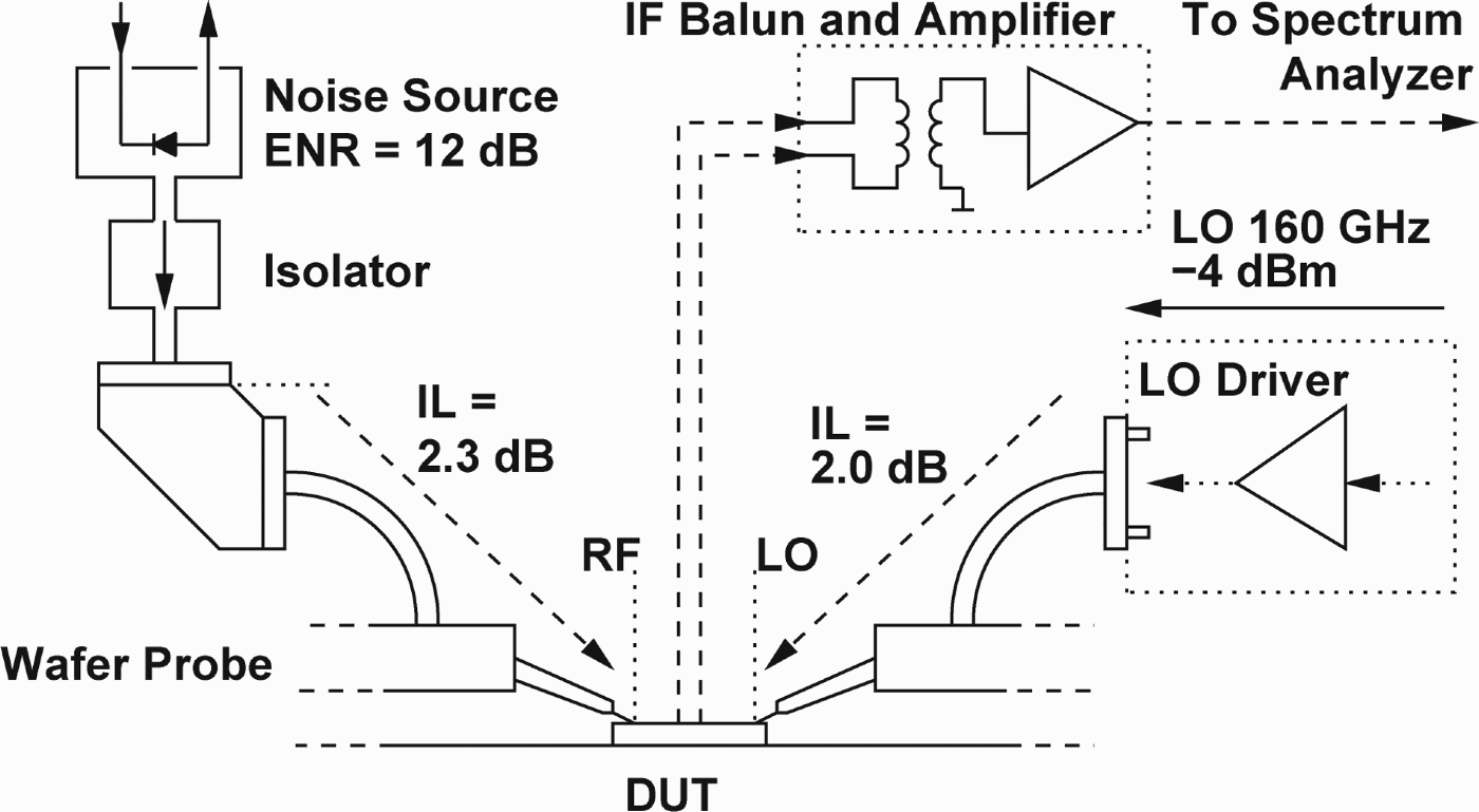
Noise-figure and conversion-gain measurements have been performed with the Y-factor method using the setup shown in Fig. 10. A calibrated IMPATT-based noise source with a 12-dB excess noise ratio (ENR) was used to provide the hot/cold input noise through a waveguide bend and the wafer probe. The measurements have been corrected for the 2.3-dB insertion loss presented by the wafer probe at the input the downconverter. Measurements of reflective standards provided by the probe manufacturer were used for this insertion-loss correction. At the output, an IF balun transformer and a low-noise buffer amplifier with 35-dB gain and a 1-dB noise figure are used to feed the IF signal to a spectrum analyzer. The spectrum analyzer is used to observe the Y-factor as well as the absolute noise spectral density at the 1-GHz IF frequency. Since the image frequency falls within the LNA bandwidth, the measured NF corresponds to the double-sideband (DSB) NF. A synthesized external signal generator equipped with a D-band source module and three cascaded D-band amplifiers with a 140-GHz gain peak provides −4 dBm of 160-GHz LO power, thus yielding −8 dBm at the mixer core LO input after the probe and on-chip balun losses.

Fig. 10. Y-factor noise-figure and conversion-gain measurement setup. A calibrated IMPATT noise source is used as the hot standard.
Figure 11 presents the measured and simulated conversion gain including the 2-dB losses of the RF pad and the input balun. A maximum conversion gain of 27 dB is obtained at 156 GHz, which is in close agreement with the sum of the LNA and mixer simulated gain at the −8 dBm LO-drive level. The output power of the 140-GHz LO-drive amplifiers in the measurement setup drops rapidly above 160 GHz. This leads to a reduced conversion gain of the mixer.

Fig. 11. Measured and simulated conversion gain including the 2-dB losses of the on-chip auxiliary RF-input balun and pad.
The measured and simulated noise figure is shown in Fig. 12. The 160-GHz measured DSB noise figure is 8.9 dB. As in the case of the conversion gain, the 2-dB losses of the RF pad and the input balun have not been de-embedded. Hence, the measurement corresponds to a NF of close to 6.9 dB at the LNA differential input terminals. The reduced LO-drive power above 160 GHz and the associated drop in the conversion gain of the mixer results in a corresponding increase of the cascaded system noise figure compared to the simulated value.

Fig. 12. Measured and simulated NF including the 2-dB losses of the input pad and the on-chip auxiliary balun in front of the LNA.
The lower NF obtained in the measurements compared to the simulations can be explained by the characterization of a wafer with an increased collector doping compared to the reference B3T devices used for the model development. The f t improvement obtained by this process modification, described in Section II.A, also reduces the NFmin. In Fig. 12 it can also be noted that the NF increases with decreasing conversion gain, thus indicating that the cascaded system NF is limited by high mixer noise when sufficient LO power is not available.
C) Input compression point
Input compression measurements have been performed using a CW-signal generated by a mmWave source module with a variable output power. An Erickson calorimeter and a harmonic mixer were used to calibrate the input power to the DUT.
The results of input compression measurement of the downconverter performed at a 160-GHz input frequency are shown in Fig. 13 together with simulation data. The high-gain LNA causes the mixer to reach the −1-dB compression point at an input power of -30 dBm and a drop is seen in the IF-output power with input signals above −25 dBm. This effect is likely caused by the low LO-pumping power available from the test equipment, which causes a strong RF-input signal to shift the operating point of the mixer quad devices.

Fig. 13. Measured input compression point of the 160-GHz downconverter.
The total current consumption of the implemented downconverter is 48 mA from a 3.3-V supply, thus corresponding to 160 mW of dc power. Half of the power is consumed by the IF-output buffers and the non-optimized biasing networks. Hence, a power consumption below 100 mW per channel can likely be obtained in an optimized multi-channel array design.
V. CONCLUSION
A 160-GHz low-noise downconversion receiver front-end with a measured 25 dB conversion gain and 8.9-dB DSB cascaded system noise figure at an input frequency of 160 GHz has been demonstrated in an engineering version of an advanced SiGe BiCMOS technology. In its intended differential-input configuration, it is expected to yield a noise figure below 7 dB due to the elimination of the losses of the auxiliary input balun used for characterization purposes in this work. The achieved 160-GHz system noise performance is similar to the 7.5-dB single-channel NF of the 60-GHz array receivers implemented in a commercial f t = 200-GHz SiGe BiCMOS technology [Reference Reynolds7]. The downconverter can be extended to an image-reject or I/Q architecture by the addition of a LO hybrid and a second mixer core. The compact layout, low dc-power consumption and the low LO-drive requirements make the design well suited for monolithic integration of multiple channels in focal-plane or phased-array configurations.
ACKNOWLEDGEMENTS
This work was supported by the European Commission under the project DOTFIVE (no. 216110).
 Erik Öjefors received his M.Sc. degree in engineering physics and his Ph.D. degree in microwave technology from Uppsala University, Sweden, in 2000 and 2006, respectively. In 2007 he joined the Institute of High-Frequency and Quantum Electronics at the University of Siegen, Germany. Since 2008, he is with the Institute for High-frequency and Communication Technology at the University of Wuppertal, Germany.
 Franck Pourchon was born in Villeurbanne, France, in 1974. He received the M.S degree in physics from the Ecole Nationale Superieure de Physique de Grenoble, France, in 1999. The same year, he has joined the Technology R&D department of Alcatel Microelectronics (now ON-Semiconductor) in Belgium where he was involved in technology modeling for DMOS and BiCMOS technologies development. In 2001, he joined the Device Modeling group of STMicroelectronics Crolles, France. He is currently in charge of transistor modeling for bipolar devices of advanced BiCMOS technologies.
 Pascal Chevalier received the engineering degree in science of materials from the University School of Engineers of Lille, France, in 1994 and the Ph.D. degree in electronics from the University of Lille in 1998. His doctoral research dealt with thedevelopment of 0.1-µm InP-based HEMT technologies. He joined Alcatel Microelectronics, Oudenaarde, Belgium, in 1999, where he contributed to the start of RF BiCMOS and led the development of SiGe BiCMOS technologies. In 2002, he joined STMicroelectronics, Crolles, France, to develop high-speed SiGe HBTs for millimeter-wave BiCMOS. He is presently a staff engineer in charge of the development of advanced RF and millimeter-wave devices. Dr Chevalier has authored or co-authored more than 100 technical journal papers and conference publications. He has been the chair of the process technology subcommittee for the IEEE Bipolar/BiCMOS Circuits and Technology Meeting. He belongs to the wireless working group of the ITRS of which he leads the Bipolar subgroup.
 Ullrich R. Pfeiffer received the diploma degree in physics and the Ph.D. in physics from the University of Heidelberg, Germany, in 1996 and 1999, respectively. In 1997 he worked as a research fellow at the Rutherford Appleton Laboratory, Oxfordshire England. In 2000 his research was based on real-time electronics for a particle physics experiment at the European Organization for Nuclear Research (CERN), Switzerland. From 2001 to 2006 he was with the IBM T.J. Watson Research Center where his research involved RF circuit design, power amplifier design at 60GHz and 77GHz, high-frequency modeling and packaging for millimeter-wave communication systems. In 2007 he lead the THz electronics group at the Institute of High-Frequency and Quantum Electronicsat the University of Siegen, Germany. Since 2008 he holds the High-frequency and Communication Technology chair at the University of Wuppertal, Germany.