


I. INTRODUCTION AND MOTIVATION
Advances in silicon semiconductor technology and the proliferation of automotive radar sensors has brought a new drive to small and highly integrated low-cost radar sensors, which can be used for speed and distance measurement in commercial and consumer applications.
Frequencies in the millimeter wave range above 100 GHz are especially interesting, as they allow small circuit and antennas sizes. From a practical point of view, the D-band (90–140 GHz) poses a good compromise between the available circuit performance in silicon technology and practical antenna size. In particular, the 122–123 GHz ISM band was designated to be used for short-range devices (SRD) in a large number of countries, worldwide.
Several integrated 122 GHz radar sensors have been published in recent years [Reference Girma, Hasch, Sarkas, Voinigescu and Zwick1–Reference Girma3]. However, a complete sensor module, comprising a fully integrated sensor frontend with angle, distance, and speed measurement capabilities has not been published to date.
To address this issue, a dual-channel single-chip SiGe-BiCMOS transceiver integrating two on-chip antennas for angular measurement was developed. The monolithically integrated radar includes a voltage controlled oscillator (VCO), frequency doublers, power amplifiers (PAs), low-noise amplifiers (LNAs), and sub-harmonic mixers (SHMs). The chip is implemented in a 130 nm SiGe-BiCMOS process with f T /f max = 280/300 GHz and dissipates 450 mW.
II. PHASE MONOPULSE FUNCTIONAL PRINCIPLE
The principle of monopulse phase direction finding lies in the reception of signals reflected from a target simultaneously along several independent receiving channels with the subsequent comparison of their parameters. Figure 1 shows a schematic representation of the angle measurement principle with two parallel RX channels. Assume two antenna separated by a distance d, with a wavefront incident angle θ, and then the extra path, Δl, the signal must travel between RX1 and RX2 results in a phase difference, ΔΦ, between the two antennas.
 $$\Delta l = d\,{\rm sin}(\theta ).$$
The path difference results in a phase difference Δϕ between the signals from the two antennas:
 $$\Delta \Phi = 2\pi \Delta l/\lambda, $$
 $$\Delta \Phi = 2\pi d\,{\rm sin}(\theta )/\lambda. $$
This can be used to calculate the direction of arrival using:
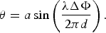 $$\theta = a\,{\rm sin}\left( {\displaystyle{{\lambda \Delta \Phi} \over {2\pi d}}} \right).$$
Owing to the azimuth position of the target, a linear phase shift can be observed in the receive signal between the consecutive antennas. The phase shift can be exploited to obtain the corresponding angle and hence the direction-of-arrival (DoA). For a distance d = λ/2 between the two antenna elements, and according to the spatial sampling theorem, azimuth angles in the range of θ = [−π/2, π/2] can be measured. For unambiguous results, the antennas should be spaced half a wavelength apart, or less.

Fig. 1. Principle of angular measurement based on phase difference in the azimuth plane.
III. TRANSCEIVER ARCHITECTURE AND CIRCUIT IMPLEMENTATION
The block diagram of the proposed transceiver is illustrated in Fig. 2. The transceiver is driven by a 60 GHz LO signal generated by a push–push oscillator to further reduce the VCO fundamental to around 30 GHz. A divide-by-16 chain, at approximately 3.8 GHz, is provided to an off-chip phase-locked loop (PLL), to lock the VCO to a stable reference frequency and modulate the transmit signal in frequency-modulated continuous-wave (FMCW) mode. Each of the two identical transmit channels include, a frequency doubler, a coupler and bi-directional power detector (PD) to measure the absolute output-power and antenna matching. This configuration allows us to fully characterize the transmitter path up to the antenna by using DC measurements. Two antennas are integrated to transmit and receive a signal simultaneously, in which a directional coupler that isolates the transmitted signal and the received signal reflected by the target.

Fig. 2. Block diagram of the realized transceiver chip.
In the receiver chain, the LNAs are followed by two sub-harmonically pumped mixers, to mix the receive and LO signal to baseband. The two passive SHMs are driven by the same 60 GHz LO signal as the input of the frequency doubler. The baseband signals are further amplified by a pair of variable-gain amplifiers (VGA). The detail of circuit level design and analysis of the building blocks are presented in [Reference Debski, Winkler, Sun, Marinkovic, Borngraeber and Scheytt6, Reference Winkler10, Reference Winkler, Debski, Schmalz, Borngraeber and Scheytt11]. The digital control block consists of serial-peripheral-interface (SPI) core with register files are used to control the on-chip circuits, such as VCO coarse tuning, multiplexer output control, gain control of the PA, LNA as well as VGAs. The main system-level parameters are summarized in Table 1.
Table 1. Summary of realized radar sensor system-level parameters.

IV. ANTENNA DESIGN AND IMPLEMENTATION
One of the main benefits of designing transceivers operating above 100 GHz is the reduced antenna size. It thus becomes feasible to integrate the antenna on the same chip with the transceiver, thereby avoiding lossy mm-wave transitions between the chip and the package.
A) On-chip antenna concept
On-chip antennas integrated on silicon technologies have been investigated for many years to provide highly integrated and low-cost solution for short-range applications in the millimeter-wave bands [Reference Hasch, Wostradowski, Gaier and Hansen8, Reference Nezhad-Ahmadi, Fakharzadeh, Biglarbegian and Safavi-Naeini9, Reference Zevallos Luna, Dussopt and Siligaris12]. The main benefit of the on-chip integration is to avoid any interconnection of high-frequency signals, which necessitate complex and expensive technologies. However, the drawbacks come from the poor antenna performance obtained from the low-resistive silicon. The antenna, which converts RF power from the circuits to electromagnetic (EM) radiation, finds low-resistive path through the substrate and leads to gain degradation. The second drawback of implementing antenna in silicon-based technologies is its high-dielectric constant (ε r ≈ 11.7), causing most of the power to be confined in the substrate instead of being radiated into free space, further degrading the radiation efficiency. To counteract this behavior, a number of techniques have been deployed to improve the radiation efficiency of on-chip antennas by redirecting the power coupled into the substrate, as in [Reference Chen, Wang, Yao and Heydari4, Reference Sarkas, Hasch, Balteanu and Voinigescu5].
The proposed antenna configuration consists of a parasitic resonator placed on top of the radio chip excited by a shorted patch antenna implemented in the back-end layer stack, a similar approach as in [Reference Girma, Hasch, Sarkas, Voinigescu and Zwick1]. Figure 3 presents the layout of the 122 GHz electromagnetically coupled on-chip microstrip antennas. The three-bottom metal layers (M1–M3) are shunted together and act as the ground plane for the antenna, which isolates the antenna from the lossy silicon substrate. The quarter wavelength patch is located at the top-metal layer (TM2). The simulated directivity for two antenna elements in cumulative is D ≈ 9.2 dBi and the simulated gain is G = 8.6 dBi ± 0.7 dB at 120–123 GHz (G = εD, efficiency ε = 60 ± 8%). The simulated efficiency of the two antennas with and without the quartz-resonator is shown in Fig. 4. The spacing between the two antennas is 0.5λ at 122 GHz. The mutual coupling between the antennas were simulated using the three-dimensional (3D) EM simulator, CST to be <−25 dB at 120–123 GHz.

Fig. 3. Antenna Model : (a) An electromagnetically coupled quartz-glass antenna placed on the top of the silicon chip, (b). 3D CST-Microwave studio simulation model.

Fig. 4. Simulation results of antenna efficiency with and without quartz glass.
B) Packaging
Radar sensors that meet both cost and performance expectations also require complementary advances in how the ICs are packaged and assembled, which must be both reliable and cost-effective. This is a key element in the ability to produce truly low-cost millimeter-wave systems. Quad-flat no-leads (QFN) packages are of particular interest as they can have an exposed pad at the bottom side of the package, thus offering both a local electrical and thermal ground. They are also compatible with automated assembly techniques. The realized radar transceiver is packaged using a wire-bonding technology in a 5 × 5 mm2 open cavity QFN package, as shown in Fig. 5. As all millimeter wave signals are routed inside the package, only direct current (DC) and signals with a frequency of less than 3.8 GHz need to be conducted through the package leads.

Fig. 5. Photographs of the SMD radar, 5 × 5 mm2 [Reference Girma, Hasch, Gonser, Sun and Zwick7].
The radiation pattern measurements are performed in an anechoic chamber, by rotating the radar sensor board to scan the half-sphere around the measuring antenna. In this measurement scenario, the radar sensor is used as a transmitter and a standard gain horn antenna as a receiver in the far-field region. The antenna's measured and simulated radiation patterns are shown in Figs 6(a) and 6(b), which show good agreement. This term represents the result of adding up all the radiation contributions of the two antenna elements. The theoretical and experimental radiation pattern at 121 GHz exhibits a quite good agreement in E- and H-planes. Note that both antennas are transmitting simultaneously. The theoretical radiation pattern in the E-plane is nearly omni-directional since the antenna is simulated with an infinite ground plane. Practically, the packaged antenna is soldered on a test board with a limited ground plane and several wire-bond connectors affecting the radiation at elevation angle close to the horizon.

Fig. 6. Normalized radiation patterns at a frequency of 121 GHz: (a) Measured (- -) and simulated (–) E-plane radiation pattern in dB, (b) Measured (- -) and simulated (–) H-plane radiation pattern in dB.
V. SENSOR HARDWARE INTEGRATION
Figure 7 shows the block diagram of the complete radar sensor module. To facilitate easier sensor module development, the sensor was split into two separate components: a baseband board and a radar board. The radar board includes the 122 GHz radar transceiver, a PLL chip for frequency control and modulation, and local power supply. The baseband board contains the analog and signal conditioning circuits, as well as an SPI interface for, for digital communication. The baseband board is mounted at the back of the radar board using standard dual-row pin headers. To allow a flexible signal processing, the digitized baseband signals are transferred to a PC via USB-Interface, which is additionally used as power supply.

Fig. 7. Block diagram of the radar module, which contains the radar board with a frequency control unit, and the base-band signal conditioning circuitry.
Figure 8 shows the printed circuit board (PCB) of the radar board. A close-up view of the sensor that is soldered onto the PCB and the quartz resonator is shown in Fig. 8(a). To protect the IC and the bond wires from environmental influences, a protecting cap with a thickness of half the guided wave length at the center frequency of 122.5 GHz was designed, as shown in Fig. 8(b). As the reflected waves at the two interfaces air-dielectric and dielectric-air effectively cancel out, the cap has a marginal effect on the antenna performance.

Fig. 8. SMD radar sensor mounted on a low-cost PCB. (a) Detailed view of the soldered sensor, (b) Sensor covered with a protecting cap.
VI. PERFORMANCE AND EXPERIMENTAL RESULTS
Different Measurements of a single-target scenario with a corner reflector have been performed in an anechoic chamber to evaluate the achievable range and angular estimation performance of the transceiver chip. A dielectric lens above the RF board provided a narrow elevation beam and an increased relative antenna gain, resulting in a better signal-to-noise ratio (SNR). While range measurements have been taken both with and without the dielectric lens, angular measurements have only been taken without the lens, as the shift of the two antenna positions against the focus point of the lens leads to divergent influences on the received phase. Additionally, the two-way antenna diagram was calculated from the received power in the same single-target scenario over different angles. The measurement setups are depicted in Fig. 9.

Fig. 9. Measurement setups for distance and angle estimations.
For all measurements, an FMCW modulation with fundamental frequency f c = 120.5 GHz, bandwidth Δf = 1500 MHz, and ramp duration T s = 10 ms was used. The sampling rate of the ADC was set to 145 kHz. Digital signal processing, controlling the parameters of the transceiver via the SPI interface, and read-in of the measurement data was performed on a standard PC.
A) Two-way antenna pattern
The mean output power of the receive mixer of a single RX channel is used as an estimate for the received power in conjunction with a reflecting target at various angles. This estimates the two-way beam pattern of the antenna, as shown in Fig. 10. The antenna characteristic determined using this method represents the combination of RX and TX antenna beam pattern. For the two-way antenna diagram, a more distinct asymmetry than in the E-plane one-way antenna diagram in Section IV can be observed.

Fig. 10. Two-way pattern obtained from the target responses.
B) Range measurement
The first range measurement was performed with a dielectric lens above the RF board and a corner reflector as target that was moved on a linear drive from 1 to 2 m in steps of 1 cm. At each position, 20 measurements have been taken to assess the reproducibility of the range measurements. The signal processing comprised detrending, windowing with a Hanning weighting function, conversion to frequency domain by fast Fourier transform (FFT) with zero padding, and calculation of estimated distance according to the frequency peak. Figure 11 shows the resulting estimation error dependent on the actual distance. The systematic error is estimated as the mean of the 20 measurements for each range. For this specific measurement example, the absolute deviation is ±3 mm.
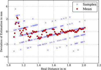
Fig. 11. Distance estimation error for single-target corner reflector and RF sensor with lens.
A second range measurement was performed without the dielectric lens and with an adapted baseband signal filtering. Here, the target was moved from 0.5 to 3 m in steps of 0.5 m. Figure 12 shows the results of this measurement series, where the error bars represent the standard deviation of the random error. Note that the lower RF power due to the missing lens required a slight modification of the analog baseband processing. The baseband signals were AC-coupled, to minimize the effect of DC offset due to the crosstalk between RX and TX channels.

Fig. 12. Distance estimation for single-target corner reflector and RF sensor without lens.
C) Azimuth angle estimation
For the evaluation of the angular estimation performance, a measurement setup with a stationary corner reflector and the radar sensor mounted on a rotating table is used as shown in Fig. 9(b). In this measurement scenario, no dielectric lens is deployed as it results in a very narrow antenna beam for angular measurements. Therefore, the same modifications as for the distance measurements without lens have been made to the analog hardware. The radar sensor is rotated from angles of −90° to +90° in steps of 5°. The angle-of-arrival is calculated by phase difference measurement of the receive channels, as described in Section II. In every position, 20 measurements have been taken to assess both the systematic and the random error, represented in the mean and standard deviation of the measurements in one specific position. This distinction is crucial, as systematic errors can be removed by calibration, while random errors remain. In Fig. 13, the results of the azimuth angle estimation using the conventional beam forming algorithm of the two channels is depicted. Here, the lengths of the error bars show the standard deviation of the random error. At wider angular position of the radar sensor, both the mean and random error of the angular estimation increase due to the decreasing SNR. This behavior results from the strongly decreased SNR at larger angles and is asymmetric in this case, in accordance to the two-way antenna diagram in Fig. 10.

Fig. 13. Estimated angular position and standard deviations determined from 20 measurements: sensor actual position on the rotation table versus estimated angle.
VII. CONCLUSION
An integrated single-chip monopulse transceiver has been realized for operation at D-band frequencies. The transceiver is based on a SiGe-BiCMOS chip with two separate integrated antennas. The SMD radar requires no external millimeter wave connections, thus enabling the assembly in a standard SMD line. Owing to the two receiving channels, angular measurement in azimuth direction is possible. These results demonstrate the potential of compact D-band radar sensor for a consumer application.
ACKNOWLEDGEMENT
The research leading to these results has received funding from the European Community’s Seventh Framework Programme [FP7/2007–2013] under grant agreement n° 248120.
 Mekdes Gebresilassie Girma received the B.Sc. degree in Electrical Engineering from the University of Mekelle, Mekelle, Ethiopia, in 2006 and the M.Sc. degree from the University of Paderborn, Paderborn, Germany, in 2010. Currently, she is working toward the Ph.D. degree in corporate research at the Robert Bosch GmbH, Stuttgart, Germany. Her research interests include the system design of millimeter-wave radar sensors.
 Markus Gonser received his Dipl.-Ing. (FH) (M.S.E.E.) degree in Electrical Engineering from University of Applied Sciences Mannheim, Germany in 2007 and the Dr.-Ing. (Ph.D.E.E.) degree from the University of Erlangen, Germany in 2011. Since then he has been working in corporate research at the Robert Bosch GmbH, Stuttgart, Germany. His research interests include simulation and measurement methods for linear electrical RF networks, radar systems, and digital signal processing.
 Andreas Frischen received his Dipl.-Ing. degree from RWTH Aachen University, Aachen, Germany, in 2012. Currently, he is working toward his Ph.D. degree at corporate research of the Robert Bosch GmbH in Stuttgart, Germany. His research interests include radar systems and signal processing.
 Jürgen Hasch received the Dipl.-Ing. degree in 1996 and his Ph.D. in 2007 from the University of Stuttgart. He is a senior expert at corporate research of the Robert Bosch GmbH in Stuttgart, Germany. His main interests are microwave and millimeter-wave sensing technologies. Dr. Hasch is a member of IEEE TC MTT-27 and VDE ITG-FA Mikrowellentechnik.
 Yaoming Sun received his B. Eng. degree, master degree, and Ph.D. degree from Xidian Uni. (Xi'an, China), Katholieke Universiteit Leuven (KUL, Leuven, Belgium) and Brandenburgische Technische Universität Cottbus (BTU, Cottbus, Germany) in 1997, 2003, and 2009, respectively. He worked in the field of mobile communication RF transceivers from 1997 to 2002 in a Xiamen-based company in China. In 2003 he worked on a Ku-band transceiver design based on a MCM technology in IMEC, Belgium. He joined the IHP microelectronics (Germany) as a scientist since 2003. He has designed and co-designed the first silicon-based 60 GHz transceiver chipset in Europe. From 2010, Dr. Sun has coordinated the design of 122 GHz mixed-signal radar chipsets in an EU project ‘SUCCESS’. He is now with Hong Kong Microsystem as technical director. His main research interests are designs of millimeter wave transceivers in a single chip for wireless communications and radar sensors.
 Thomas Zwick received the Dipl.-Ing. (M.S.E.E.) and the Dr.-Ing. (Ph.D.E.E.) degrees from the Universität Karlsruhe (TH), Germany, in 1994 and 1999, respectively. From 1994 to 2001 he was a research assistant at the Institut für Höchstfrequenztechnik und Elektronik (IHE) at the Universität Karlsruhe (TH), Germany. In February 2001, he joined IBM as research staff member at the IBM T. J. Watson Research Center, Yorktown Heights, NY, USA. From October 2004 to September 2007, Thomas Zwick was with Siemens AG, Lindau, Germany. During this period he managed the RF development team for automotive radars. In October 2007, he became a full professor at the Karlsruhe Institute of Technology (KIT), Germany. He is the director of the Institut für Hochfrequenztechnik und Elektronik (IHE) at the KIT. He is author or co-author of over 200 technical papers and 20 patents. His research topics include wave propagation, stochastic channel modeling, channel measurement techniques, material measurements, microwave techniques, millimeter wave antenna design, wireless communication, and radar system design. Dr. Zwick received over ten best paper awards on international conferences. He served on the technical program committees (TPC) of several scientific conferences. In 2013, Dr. Zwick was the general TPC Chair of the international Workshop on Antenna Technology (iWAT 2013). He was also the TPC Chair of the European Microwave Conference (EuMC) 2013. Since 2008 he has been the President of the Institute for Microwaves and Antennas (IMA). T. Zwick became selected as a distinguished microwave Lecturer for the 2013–2015 period with his lecture on ‘QFN Based Packaging Concepts for Millimeter-Wave Transceivers’.


