


I. INTRODUCTION
Many recent handsets, such as smart phones, have transceivers for multiple wireless standards. Multiple power amplifiers (PAs) to accommodate different frequencies, bandwidths, peak output powers, and modulation schemes are required, at the cost of large area. An important research objective is to develop a single transmitter that can work in multi-standard operation with high efficiency.
A digitally-assisted PA is one of the potential solutions to realize a multiband and multimode transmitter [Reference Eloranta, Seppinen, Kallioinen, Saarela and Parssinen1, Reference Choi2]. Co-design of digital signal processing (DSP) algorithms and PA circuits can lead to improved efficiency and linearity in multiple conditions. It is attractive to integrate both DSP and PA into one die because many control lines operating with high clock rate can be readily accommodated and it is relatively easy to manage delay time between control lines, compared with multi-chip solutions.
In the previous work, we have demonstrated a digitally-driven polar modulation transmitter at 0.75 GHz [Reference Nakatani, Rode, Kimball, Larson and Asbeck3, Reference Nakatani, Rode, Kimball, Larson and Asbeck4], in which a watt-class current-mode class-D (CMCD) CMOS PA [Reference Nakatani, Rode, Kimball, Larson, Asbeck and Osman5] with 9 V breakdown voltage stacked-field-effect transister (FET) combinations and a 47 MHz buck converter were employed. A WCDMA waveform was encoded using digital pulse width modulation (DPWM) [Reference Peterchev and Sanders6] with a digital pre-emphasis synchronized by a 3 GHz clock. Digital control signals were fed from an external instrument. An overall efficiency of 26.5% was achieved while maintaining ACLRs within 3GPP specifications at 24 dBm average output power.
The next challenge is to realize multiband operation. Several multiband CMOS PAs have been reported [Reference Neo7–Reference Kim, Kim, Son, Oh and Park11]. In [Reference Neo7], high-Q varactor-based tunable matching networks are integrated and output power of 27–28 dBm is achieved at 0.9, 1.8, 1.9, and 2.0 GHz. In [Reference Presti, Carrara, Scuderi, Asbeck and Palmisano8], fixed off-chip matching networks of a class-E amplifier are used to cover 0.8–2.0 GHz. In [Reference Imanishi, Okada and Matsuzawa9], band-switching feedback and output resonator circuits adjust the output impedance to 50 Ω over 0.9–3.0 GHz. In [Reference Hur, Lee, Lee, Lim and Laskar10], by applying an integrated band-switching output capacitor of a voltage-mode class-D amplifier, a 3 dB bandwidth from 0.45–0.73 GHz with an output power of 20 dBm is achieved. In [Reference Kim, Kim, Son, Oh and Park11], a quad-band PA for 1.9, 2.3, 2.6, and 3.5 GHz is implemented by changing the number of active transistors. However, their peak output powers were less than 28 dBm. Over 30 dBm, multiband CMOS PAs are desirable for cell phone applications.
In this work, we demonstrate a multiband digital polar transmitter using a watt-class CMCD CMOS PA with a band-switching resonator [Reference Nakatani, Kimball, Larson and Asbeck12]. A band-switching capacitor (BSC) with a 9 V breakdown voltage is used to change resonance frequency since it is difficult to cover the entire band using a fixed value inductor-capacitor (LC) resonator. A 0.5–2.1 GHz doughnut-shaped Guanella reverse balun [Reference Nakatani, Rode, Kimball, Larson and Asbeck4, Reference Nakatani, Rode, Kimball, Larson, Asbeck and Osman5] is employed as an output balun. The continuous wave (CW) output powers and overall efficiencies of the transmitter are measured to be 30.2/28.9 dBm and 27.1/25.6% at the carrier frequencies of 0.85/1.75 GHz, respectively.
Another challenge of the digital polar transmitter is to provide clean output waveforms without artifacts from the use of purely digital input signals. The most prominent problem with the DPWM algorithm is the presence of clock images associated with the digital envelope input [Reference Jiang, Lopez and Maksimovic13, Reference Alimenti, Gesano, Nocito and Pezzetta14]. Many techniques to avoid clock images have been reported [Reference Tao and Fayed15–Reference Chen, Liu and Chen18]. In [Reference Tao and Fayed15], phase chopping is applied for a spur-free output. However, the technique is only useful for a constant envelope signal like Global system for mobile communications (GSM). In [Reference Qin, Guo, Park and Huang16], an auxiliary branch of an envelope modulator, which works with the opposite phase of the main branch, is connected in parallel to cancel the ripple of an output signal. However, two large output inductors are needed. In [Reference Kitchen, Deligoz, Kiaei and Bakkaloglu17] and [Reference Chen, Liu and Chen18], ΔΣ and Δ modulations and random carrier frequency modulation (RCFM) are applied to decrease peak out-of-band spurs. However, in order to meet adjacent channel leakage ratio (ACLR) specifications, ΔΣ modulation requires high average frequency, which causes large DC power consumption. Δ modulation needs an analog feedback circuit, which limits maximum bandwidth. RCFM increases the noise floor coming from quantization noise. Other dithering techniques like random pulse position modulation and random pulse width modulation [Reference Tse, Chung, Hui and So19] also have a similar trend.
In this work, a new dithered DPWM technique is demonstrated to reduce clock images and quantization noise [Reference Nakatani, Kimball, Larson and Asbeck12]. Peak spurs decrease by over 3.2/9.0 dB when average switching frequencies of the DPWM are 46/184 MHz respectively.
II. DESIGN AND ANALYSIS OF MULTIBAND CMCD PA
A) Design of variable resonator
Figure 1 shows the circuit configuration of the multiband CMCD amplifier [Reference Hung, Metzger, Zampardi, Iwamoto and Asbeck20]. The current through switch (I 1) is a square wave with the switching frequency (f c), while the voltage across each switch (V 1) is a half sine wave. A variable parallel resonator consisting of variable capacitors (C res) and inductor (L res) is used to adjust resonance frequency and for harmonic termination, and only the fundamental component of the differential voltage reaches at the load. Our CMCD PA uses a 1-to-4 balun as an appropriate tradeoff between peak voltage and output loss [Reference Nakatani, Rode, Kimball, Larson and Asbeck4].
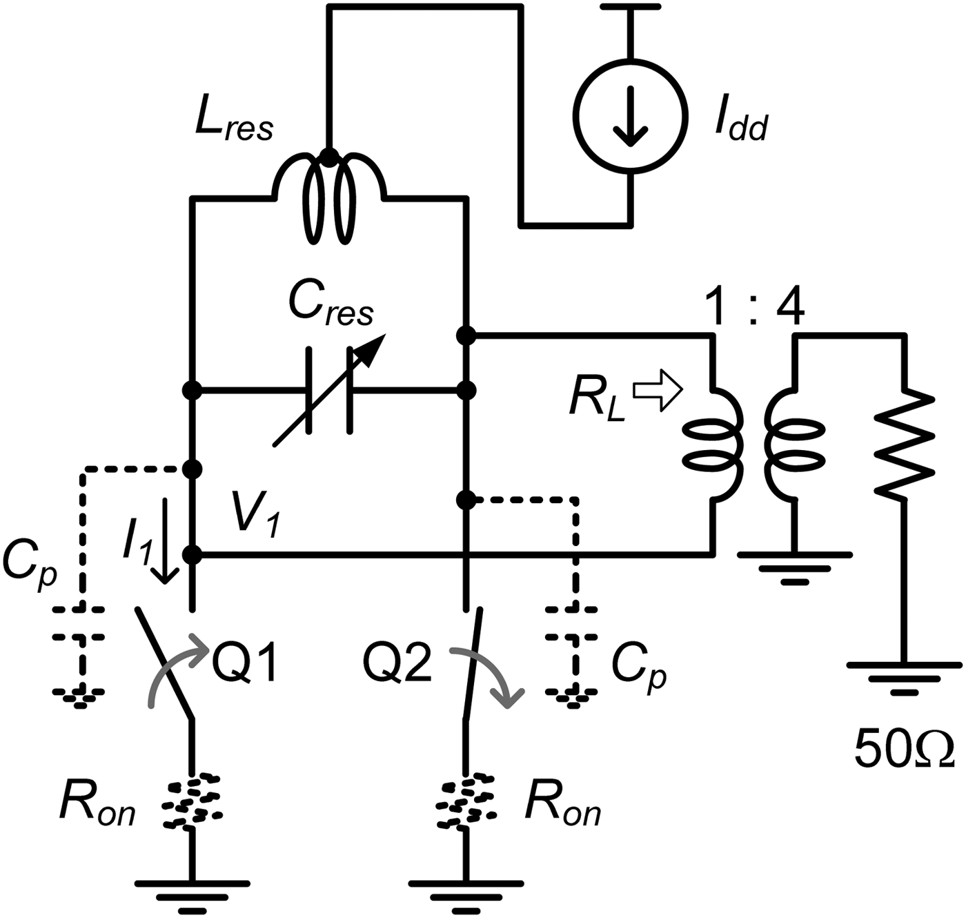
Fig. 1. Circuit configuration of the multiband CMCD amplifier.
The WCDMA frequency bands are roughly categorized into two groups: low band (0.698–0.915 GHz) and high band (1.71–1.98 GHz) excluding Band VII and XI. Here, we focus on 0.85 and 1.75 GHz as resonance frequencies of the variable resonator.
When switch Q1 is open and switch Q2 is closed, the resonator is the parallel circuit of C res, L res, and fixed parasitic capacitance between the output and ground (C p). The resonance frequency is written as
 $$f_{res} = {1 \over 2\pi \sqrt{L_{res} \lpar C_{res} + C_p\rpar }}.$$
The drain efficiency can be expressed as follows (see Appendix):
 $$\eta = {\left(1 - \displaystyle{{Q_L \over Q_u}} \right)\displaystyle{1 \over 1 + n\lpar 1\rpar ^2 Q_L^2} \over \sum\nolimits_{k = 1}^{\infty} \displaystyle{1 \over \lpar 2k - 1\rpar ^2} \displaystyle{1 \over 1 + n\lpar k\rpar ^2 Q_L^2}}\comma \; $$
where Q u and Q L are the unloaded and loaded Qs of variable resonator; n(k) = (2k − 1) f c/f res − f res/{(2k − 1) f c} (k = 1, 2, …), is a factor describing the harmonic response of the variable resonator and k designates the odd harmonic index [Reference Nakatani, Rode, Kimball, Larson and Asbeck4, Reference Hung, Metzger, Zampardi, Iwamoto and Asbeck20].
Figure 2 shows the required C res for 0.85 and 1.75 GHz and the drain efficiencies of the CMCD PA versus L res of the variable resonator calculated using equations (1) and (2). In Fig. 2, C p is assumed to be 5 pF. With increasing L res of the resonator, the area of C res can be reduced, but the required capacitance ratio between low and high band conditions increases. When L res is 0.5 nH, the required capacitance ratio is 5.6, which is lower than that of the fabricated BSC of approximately 6 as shown in the following section. In Fig. 2, unloaded quality factors of 8.5 and 7.5 at 0.85 and 1.75 GHz are used, based on the value estimated in the following section. With decreasing L res, the drain efficiencies decrease. When L res is 0.5 nH, the calculated drain efficiencies are 76 and 64%, which are lower than the optimal value (89–90%) but still high.

Fig. 2. Required capacitances and drain efficiencies of CMCD PA versus inductance of band-switching resonator (f res = f c = 0.85 GHz/1.75 GHz, Q u = 8.5/7.5).
B) Bandwidth degradation due to parasitic components
The variable resonator needs to tune the resonance frequency rather precisely because parasitic components of the PA degrade its bandwidth.
The left side of Fig. 3 shows the voltage waveform at the resonance frequency of the CMCD amplifier along with the voltage drop from the on-resistance (R on) of the stacked FET. The constant DC current (I dd) flows through R on of Q1 and Q2 alternatively. Therefore, the voltage waveform is shifted up by I ddR on from the ideal waveform. The on-resistance degrades drain efficiency although it does not change output power. Drain efficiency may be calculated from (see Appendix)

Fig. 3. Voltage waveform of CMCD amplifier with parasitic components: Effect of on-resistance of stacked FET at resonance frequency (left) and effect of parasitic capacitance where f c > f res (right).
 $$\eta = \displaystyle{\left(1 - \displaystyle{Q_L \over Q_u} \right)\displaystyle{1 \over 1 + n\lpar 1\rpar ^2 Q_L^2} \over \sum\nolimits_{k = 1}^{\infty} \displaystyle{1 \over \lpar 2k - 1\rpar ^2} \displaystyle{1 \over 1 + n\lpar k\rpar ^2 Q_L^2} + \displaystyle{\pi ^2 R_{on} \over 2R_L \left(1 - Q_L / Q_u \right)}}\comma \;$$
where R L is the load resistance of the CMCD amplifier (=12.5 Ω).
The right side of Fig. 3 shows the voltage waveform of the CMCD amplifier, for a case where the switching frequency is higher than the resonance frequency. In case that C p is zero, V 2(π) = −V 1(π). However, in case C p > 0 and f c > f res, C p at the V 1 side stores a positive charge when the phase is just below π. The capacitor is discharged to ground and V 2 starts from −V 1(π) + ΔV when the phase is just above π, where ΔV can be calculated from
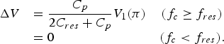 $$\matrix{\Delta V &= \displaystyle{{C_p \over 2C_{res} + C_p}} V_1 \lpar \pi \rpar \hfill &\lpar f_c \geq f_{res} \rpar \cr &= 0 \hfill &\lpar f_c\lt f_{res}\rpar .} $$
These phenomena can be expressed as adding a square wave with ΔV height to V 1 and V 2, respectively. From equation (4), the output power can be calculated from (see Appendix)
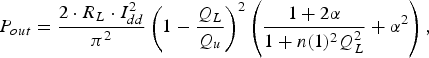 $$P_{out} = \displaystyle{{2 \cdot R_L \cdot I_{dd}^2 \over \pi ^2}} \left(1 - \displaystyle{{Q_L \over Q_u}} \right)^2 \left(\displaystyle{{1 + 2\alpha \over 1 + n\lpar 1\rpar ^2 Q_L^2}} + \alpha^2 \right)\comma \;$$
where α = 2ΔV/{I ddR L (1-Q L/Q u)} is the voltage ratio between the additional square wave and fundamental square wave of the CMCD amplifier, which is current times load resistance including the parasitic resistance of the resonator. From equations (4) and (5), the drain efficiency is calculated to be (see Appendix)
 $$\eta = \displaystyle{\left(1 - \displaystyle{Q_L \over Q_u} \right)\left(\displaystyle{1 + 2\alpha \over 1 + n\lpar 1\rpar ^2 Q_L^2} + \alpha ^2 \right)\over \sum\nolimits_{k = 1}^{\infty} \displaystyle{1 \over \lpar 2k - 1\rpar ^2} \displaystyle{1 \over 1 + n\lpar k\rpar ^2 Q_L^2} + \displaystyle{\pi^2 \over 2} \left\{\displaystyle{R_{on} \over R_L \left(1 - Q_L / Q_u \right)} + \displaystyle{\alpha \over 2} \right\}.} $$
Figure 4 shows the effect of R on and C p of CMCD PA on output power and drain efficiency, as calculated using equations (5) and (6) with f res = 0.85/1.75 GHz and Q u = 8.5/7.5, respectively; L res = 0.5 nH, I dd = 1.12 A (corresponding to the ideal output power of 35 dBm), R on = 0.5 Ω (obtained from a designed circuit in the following section), and C p = 5 pF. The figure shows that, while the maximum output power does not change appreciably, the parasitics cause narrower bandwidth, so that to maintain maximum power and efficiency, the resonant frequency must be set with high precision.

Fig. 4. Effects of R on and C p of CMCD amplifier: output power and drain efficiency (f res = 0.85 GHz/1.75 GHz, Q u = 8.5/7.5, L res = 0.5 nH, I dd = 1.12 A).
III. CIRCUIT DESIGN OF MULTIBAND DIGITAL POLAR TRANSMITTER
Figure 5(a) shows the circuit schematic of the overall transmitter, which consists of a CMCD PA and a buck converter. Similar to [Reference Nakatani, Rode, Kimball, Larson and Asbeck3, Reference Nakatani, Rode, Kimball, Larson and Asbeck4], these circuits are fabricated as two individual chips. A digitally modulated pulse signal is applied to the input AMin to provide amplitude-modulation (AM) and a differential radio frequency (RF) phase-modulation (PM) signal is supplied to PMin+ and PMin−. A differential modulated signal is delivered from the CMCD PA and a Guanella reverse balun is provided on the PCB for differential-to-single and 1-to-4 impedance conversion.

Fig. 5. (a) Circuit schematic of multiband digital polar transmitter with band-switching resonator and (b) simulated output power over frequency with different settings of band-switching resonator.
The CMCD PA contains not only a driver stage and stacked switching stage, but also BSCs and bond wire inductors, which work together as a band-switching resonator. In order to provide a switch control voltage independent of instantaneous power supply voltage, the switch is inserted between two capacitors. When the switch is closed, the capacitors dominate resonance frequency. When the switch is open, the frequency is decided by the off-capacitance of the switch. Since the switches need to tolerate 9 V peak voltage [Reference Nakatani, Rode, Kimball, Larson and Asbeck3, Reference Nakatani, Rode, Kimball, Larson and Asbeck4], two 3.3 V NMOSFETs are connected in series. In order to reduce off-capacitance to achieve wide frequency range, 3.3 V is supplied to drain, source and body, with gate at 0 V. In our design, the BSCs consist of 64 cells (21–74 pF) including C p. The number of closed BSCs is binary-controlled from outside of the chip to cover the entire band. As shown in the following section, measured unloaded Qs for the BSCs are 12 (all switches are closed, 0.85 GHz) and 9 (all switches are open, 1.75 GHz).
Three parallel bond wires are used as inductors to achieve a high unloaded Q. The total inductance is around 0.5 nH. The unloaded Qs estimated using the ADS bond wire model are 31 (0.85 GHz) and 45 (1.75 GHz), respectively. From these, the unloaded Qs of the band-switching resonator are 8.5 (0.85 GHz) and 7.5 (1.75 GHz), which limit system efficiency.
The buck converter contains a dead-time generator, 1.8 V-to-3.3 V level shifters, 8-stage drivers and final inverter. In order to reduce shoot-through current and switching loss, 90/150 psec dead times are provided at the rising/falling edges of the output voltage, respectively. The DC voltage of the driver and final stages are 3.3 V. Measurements of the buck converter alone showed efficiencies of 84/76% with 47/188 MHz switching frequencies, respectively, for a duty cycle of 87.5%.
Figure 5(b) shows the simulated output power versus frequency under ideal conditions when the number of BSCs turned on is 64 (C64), 32 (C32), 16 (C16), 8 (C8), and 0 (C0). The supplied DC current is 1.12 A, as required for ideal 35 dBm peak output power. Multiple bands can be covered using the proposed configuration and the total 3 dB bandwidth is simulated to be 1.15 GHz (0.75–1.9 GHz).
Figure 6 shows the die photos for PA and buck converter chips. Both chips were fabricated using the L-Foundry 0.15 µm RF CMOS process containing six nominal and one 6 µm thick Al metal layers. The die sizes are 1.7 × 1.5 mm2 (CMCD) and 1.39 × 1.38 mm2 (buck converter), respectively. The CMCD PA chip has extra pads for the bond wire inductor. The length of each wire is around 2.3 mm (90 mil).

Fig. 6. Chip photos of digital polar transmitter. (a) CMCD PA (1.7 mm × 1.5 mm) and (b) buck converter (1.39 mm × 1.38 mm).
IV. SPURIOUS SIGNAL REDUCTION FOR DIGITAL PULSE WIDTH MODULATION
To reduce the peak amplitude of spurious associated with the envelope clock replicas, RCFM [Reference Chen, Liu and Chen18] is one of the good candidates, in which switching between different clock frequencies randomly for the DPWM signal is used to reduce the peak amplitude of the spurs. However, the conventional RCFM increases the amount of noise compared with DPWM due to time quantization errors, especially in adjacent channels.
In order to reduce the peak amplitude of spurs without increasing near band noise, a new approach to carrier frequency modulation is proposed, whose principle is presented in Figs 7(a) and 7(b). If DPWM, whose period of pulses is fixed, is used, only a limited number of amplitudes can be selected (e.g., 2, 3, 4, and 5 are shown in Fig. 7(a)). Even if RCFM is applied, a large time quantization error is occasionally shown, when the period is short (e.g., the period is 2 and the required output level is 0.75), and the resulting noise is spread over frequency. However, if these periods can be selected appropriately in accordance with the required output level, the time quantization error can be reduced (e.g., when the required output level is 0.75, a period of 4 and a width of 3 are selected). As a result the equivalent number of timing bits increases (except for the first and last steps) as shown in Fig. 7(a).

Fig. 7. (a, b) MQED principle, and (c) schematic diagram of polar modulator for MQED.
Furthermore, even if two combinations of period and width have same width/period value (e.g., 2/4 and 4/8), their timing is in general different at the center of each period, and appropriate choices can result in a reduced quantization error. For example, Fig. 7(b) shows a representative required envelope signal, along with output pulses with the periods of 4 and 8 that could be chosen to encode it. The width/period for both pulse waveforms are 0.5. The quantities e(4) and e(8) are the errors between the required envelope signal and 0.5 at the centers of the pulses. In this case, it would be more accurate to select a period of 4 because e(4) is smaller than e(8).
Thus, if the pulse width and period whose ratio is nearest to the required envelope signal is selected every time, the near-band noise should be reduced. This approach, termed minimum quantization error dithering (MQED)Footnote 1 results in a continuous variation in the clock frequency used to represent the envelop signals, when the input is a modulated signal such as WCDMA. This technique spreads out the clock spurs, decreases the peak spur and reduces errors due to quantization.
Figure 7(c) shows the block diagram of the digital polar modulator employing the MQED technique. For this work, these digital functions are emulated using Matlab. The Matlab signals are subsequently uploaded to a pulse pattern generator, operating with the clock frequency (f 0) for the AM signal. The PM signal is generated based on Matlab inputs transferred to an arbitrary waveform generator and a vector signal generator. The input IQ data is first converted to polar format, and the PM carrier signal is generated using an 8 bit digital-to-analog converter (DAC) and analog quadrature modulator. The clock frequency of the DAC is f 0/64 due to the limitation of the instrument used.
AM data is pre-emphasized and quantized by using several pulse periods (M p) ranging from 2Nb − 2Nb−2 + 1 to 2Nb + 2Nb−2 − 1, N b = 1, 2, … . Here, N b is the average number of bits of DPWM. After that, the residual quantization errors (e) are calculated using all sets of pulse width (W p) and M p. Finally, the set of W p and M p with minimum e is selected and the PWM pattern is generated from them. In addition, the minimum e is fed back for noise shaping.
To evaluate the proposed modulation technique, the spectra of the ideal PA outputs are simulated using Matlab; MQED, DPWM, and 1bit DSM is applied. WCDMA modulation (hybrid phase shift keying: HPSK) with 3.3 dB PAR is chosen as the modulation to be represented. The source clock frequency, f 0, is 2949.12 MHz. The carrier frequency, f c, is 1.75 GHz and the RX band is 1.84 GHz (selected to correspond to UMTS band III). Ideal CMCD PA and buck converter models with 6.9 dB loss at the output are assumed, in order to match the measured power. To avoid the effect of the clock image in the PM path, a 750 MHz clock frequency is used for the PM signal. Figure 8 shows the simulated results for the case where the average switching frequency of the buck converter (f sw_ave), is constrained to be lower than 50 MHz. Figure 8(a) shows spectra with 20 MHz span; (b) shows spectra with 500 MHz span; and (c) is ACLR2 and RX band noise versus average output power. For MQED and DPWM, N b = 6 has been used; for 1bit DSM 117.965 MHz (under-clocked) was chosen in order to maintain f sw_ave < 50 MHz, corresponding to almost same peak DC power consumption of the buck converter as the average output power is swept.

Fig. 8. (a, b) Simulated spectra with 40 MHz/500 MHz span; (c) ALCR2 and Rx band noise of UMTS band III (95 MHz offset) of polar transmitter when f sw_ave < 50 MHz. (P out = 20 dBm, f c = 1.75 GHz).
Figure 8(a) shows that the near band noise of MQED is higher than that of DPWM due to noise spread effect of the dithering, at output power of 20 dBm. However, the MQED keeps the near band noise lower over a wider range of average output power by increasing the effective number of bits as shown in Fig. 8(c), where ACLR2 (whose specification is harder to meet than ACLR1) is plotted. The noise of the 1 bit DSM is much higher due to under-clocking. The trend of the noise far away from the carrier frequency is different among the three modulation approaches. The RX band noise of UMTS band III, which is located at 95 MHz higher than the carrier frequency, is considered here as an example. From Fig. 8(b), the RX band noise of the MQED is lower than that of DPWM, but higher than that of the 1 bit DSM because the second images of the average switching frequency show up in the RX band. Even if the average switching frequency is adjusted for the RX band to fall between the images, the noise level of the MQED is higher than −100 dBm/Hz. In Fig. 8(c), the RX band noise of the MQED is found to be about 7 dB higher than that of 1 bit DSM. This is because the MQED algorithm tends to spread the quantization error effects away from average switching frequency into neighboring spectral regions. This suggests that with MQED the noise level should be very low if the RX band is inside the first images.
Figure 9 shows the simulated output spectra and the average output power dependence of the noise levels when the average switching frequency is constrained to be less than 200 MHz (and thus higher than for Fig. 8). This places the RX band within the first images. N b (the average number of bits of the MQED and DPWM) is decreased to 4 and f 0 of the 1 bit DSM is scaled to be 491.52 MHz. From Figs 9(a) and 9(c), the ACLRs of the MQED are lower than for the other cases in a 0–30 dBm average output power dynamic range.

Fig. 9. (a, b) Simulated spectra in 40 MHz/500 MHz span; (c) ALCR2 and Rx band noise of UMTS band III (95 MHz offset) of polar transmitter when f sw_ave < 200 MHz. (P out = 20 dBm, f c = 1.75 GHz).
From Figs 9(b) and 9(c), the RX band noise of the MQED and DPWM are reduced to be −98 dBm/Hz or lower although that of 1 bit DSM is still around −90 dBm/Hz. In this case, the big difference between the MQED and DPWM is spurs. Peak spurs are improved by 7–9 dB using the MQED and the requirement for the duplexer can be relaxed.
V. EXPERIMENTAL RESULTS
A) Measured results of band-switching capacitor cell and CMCD power amplifier
Figure 10 shows the measured capacitances and Qs of the BSC cell with the switch closed and open (when the one port is grounded). The number of unit cells is eight for on-wafer evaluation and the parasitics of the pads are de-embedded. From these results, the capacitances are 7.7 pF (closed, 0.85 GHz) and 1.3 pF (open, 1.75 GHz) and the Qs are 12 and 9, respectively, as mentioned in the previous section. From equation (1), the resonance frequency is decided by the capacitances although actually they include shunt capacitances between the bottom plate of the MIM capacitor and the ground, which are 0.5 pF (0.85 GHz) and 0.3 pF (1.75 GHz).

Fig. 10. Measured characteristics of 9 V BSC cells: capacitance and Q (the number of unit cell is 8).
Figure 11 shows the CW measured and simulated output power and “driver + final efficiency”, which is defined as the ratio between the output power and the DC power dissipation of the driver and final stages, of the CMCD PA module (with external power supply). All switched capacitances are closed for the low band and open for the high band. The DC currents are 0.5 and 1.0 A. The symbols are measured results and the lines are transient simulated results using SPICE (simulation program with integrated circuit emphasis) FET models with chip parasitic extraction, electromagnetic simulations of S-parameters of MIM capacitors, routing and pads, bond wire model, and equivalent circuits of the on-board balun. The measured results are in good agreement with the simulations. By increasing DC, the peak output powers of 31/30 dBm are achieved at 0.8/1.65 GHz, respectively, where the drain efficiencies are 35/31%, and the driver + final efficiency are 33/29% (although they are not shown in the figure).

Fig. 11. Measured and simulated CW performance of CMCD PA over frequency: output power and driver + final-stage efficiency. (symbol: measurement, line: simulation).
One of the differences between experimental results and analytical calculations presented earlier (Fig. 4) is due to the loss of the on-board balun (0.5–1.0 dB) and DC power consumption of the driver amplifier (0.1–0.3 W). In addition, C p of the fabricated chip is actually around 11 pF instead of 5 pF. Therefore, the resonance frequency of the output resonator is shifted to a lower frequency compared with Fig. 4. Even if these are taken into account, a discrepancy remains between the measured and calculated efficiencies in the high band. One of the possible reasons is high frequency parasitic resistance of the 6 µm thick Al metal due to skin and proximity effects.
B) Measured results of multiband digital polar transmitter
1) SINGLE-TONE MEASUREMENT
Figure 12 shows the measured frequency dependence of output power and overall efficiency with 50 and 75% duty cycle and 47 MHz fixed clock DPWM (f 0 = 3000 MHz, N b = 6). The DPWM signal was generated from the pulse pattern generator, and the RF carrier signal (without PM) was applied from the vector signal generator. The numbers of closed BSC cells are 64 (C64), 32 (C32), 16 (C16), 8 (C8), and 0 (C0) for different cases. DC power dissipations of the buck converter and of the driver stage are included in the overall efficiency. By adjusting the resonance frequency of the CMCD, the output power is 23.5–26.1 dBm in the 0.7–1.8 GHz range at 50% duty cycle. With increasing frequency, the overall efficiency decreases due to the power consumption of the driver stage. When the duty cycle is 75%, the output power increases by approximately 29 dBm and the overall efficiency becomes 23–28%.

Fig. 12. Measured CW performance of digital polar transmitter over frequency: output power and overall efficiency (f sw_ave = 47 MHz, f 0 = 3000 MHz, N b = 6).
Figure 13 shows (a) the output power and (b) the overall efficiency at 0.85 GHz (C64 between Band V and Band VIII) and 1.75 GHz (C0, Band III) when the duty cycle of DPWM is swept. The envelope modulation is generated based on f sw_ave of DPWM = 47 MHz (N b = 6) and 188 MHz (N b = 4) with f 0 = 3000 MHz. Ideal output power (corresponding to the CMCD with external source) is also shown for reference. In f sw_ave = 47 MHz, the output power and overall efficiency are 30.2/28.9 dBm and 27.1/25.6% respectively at 87.5% duty cycle. The peak PAE drops to 24.5/18.3% due to 20.0/23.5 dBm external input power required, as needed to maintain proper switching operation of the CMCD in the test-bench, although in a realistic application scenario the input power would be considerably lower, since it would come from an on-chip digital buffer.

Fig. 13. Measured CW power and efficiency of digital polar transmitter at 0.85/1.75 GHz: (a) output power and (b) overall efficiency when f sw_ave = 47/188 MHz (f 0 = 3000 MHz, N b = 6/4).
When f sw_ave increases, the linearity of the output power is degraded because the buck converter cannot deal with very narrow pulses, the peak overall efficiencies are 24/22% respectively at 75% duty cycle. There is a trade-off between linearity/efficiency and RX band noise/peak spurs, as discussed in the previous section.
2) HPSK (WCDMA) MODULATION PERFORMANCE
Figure 14 shows the average output power dependence of the ACLR and overall efficiency (a, c) at 0.85 GHz using C64 and (b, d) at 1.75 GHz using C0. The PAR of the modulation signal is 3.3 dB. In the measurement, no dithering is applied for the DPWM; f sw_ave for the DPWM are (a, b) 46.08 MHz (N b = 6) and (c, d) 184.32 MHz (N b = 4) with f 0 = 2949.12 MHz. Baseband I Q signals with 46.1 MHz clock frequency are applied from the arbitrary waveform generator to the vector signal generator for the PM signal. From Figs 14(a) and 14(b), the ACLRs are within 3GPP specifications at 0.85 GHz in the range 10 to 26 dBm, and from 12 to 20 dBm at 1.75 GHz without AM–AM and AM–PM digital predistortion (DPD). The cause of non-linearity in the high band is largely the non-linearity of the switching stage parasitic capacitance. In the low band, the capacitance of the BSC (which is linear) is relatively large and mitigates the shift of the resonance frequency of the PA for low instantaneous output power. The peak overall efficiencies are 26 and 19% at 26 dBm/0.85 GHz and 25 dBm/1.75 GHz, respectively.

Fig. 14. Measured ACLR of transmitter with WCDMA signals: (a) C64, f c = 0.85 GHz, f sw_ave = 46 MHz, (b) C0, f c = 1.75 GHz, f sw_ave = 46 MHz, (c) C64, f c = 0.85 GHz, f sw_ave = 184 MHz, (d) C0, f c = 1.75 GHz, f sw_ave = 184 MHz (DPWM, f 0 = 2949.12 MHz, N b = 6/4).
In Figs 14(c) and 14(d), for high values of average switching frequency, the linearity is degraded due to the limitations of the buck converter as shown in Fig. 13. DPD may help to improve the ACLR in the wide output power range. The peak overall efficiencies are 21 and 16% at 26 dBm/0.85 GHz and 24 dBm/1.75 GHz, respectively.
Figure 15 shows the measured spectrum with (a, b) 40 MHz span and (c, d) 500 MHz span, for different envelope modulation switching rates: (a, c) 46.08 MHz (N b = 6) and (b, d) 184.32 MHz (N b = 4). The carrier frequency is 1.75 GHz and the output power is 20 dBm. The resolution bandwidth is 3 MHz. Compared with the simulated near band spectra shown in Figs 8(a) and 9(a), there is considerable spectral regrowth caused by non-linearity of the devices which dominate the ACLRs. Therefore, the measured ACLRs for MQED encoding are almost the same as those of conventional DPWM except ACLR2s for the case where f sw_ave = 46 MHz. The ACLR2s of MQED are 1–2 dB higher due to spreading of spurious noise into the alternate channel band, although the values are within the 3GPP specification. The effect of the DPD is limited by the original signal in the measured cases, and the proposed MQED should still have some advantages.

Fig. 15. Measured spectra of the polar transmitter with DPWM and MQED modulations: (a, b) span 40 MHz f sw_ave ~ 46/184 MHz, (c, d) span 500 MHz, f sw_ave ~ 46/184 MHz. (P out = 20 dBm, f c = 1.75 GHz).
In Figs 15(c) and 15(d), measured spectra over a wider span are similar to the simulations of Fig. 8(b) and Fig. 9(b). The RX band noise values estimated for UMTS band III are <− 90/ − 100 dBm/Hz. Peak spurs from DPWM are suppressed by over 3.2/9.0 dB using 46/184 MHz switching frequencies of the buck converter. In Fig. 15(d), spurs emerge at around 46/92 MHz offset frequency from the carrier due to unexpectedly small envelope variations of the PM signal caused by experimental slew rate limitations of the instrument for IQ baseband signal generation.
VI. CONCLUSION
In this paper, a multiband digital polar modulation transmitter with a band-switching resonator has been demonstrated; a new DPWM algorithm for the AM signal to decrease clock-induced noise has been described; and an analysis of output powers and drain efficiencies of a multiband CMCD amplifier has been provided. The designed transmitter comprises of a 0.7–1.8 GHz CMCD CMOS PA with over 1 W output power, and a buck converter with over 2.5 W output power and up to 200 MHz clock rate. The MQED DPWM algorithm was introduced to reduce near band noise and peak clock images. At 0.85/1.75 GHz, 30.2/28.9 dBm CW output powers and 27.1/25.6% overall efficiency are achieved, respectively, when the duty ratio is 87.5% and the switching frequency of the buck converter is 46 MHz. As the switching frequency is increased to 184 MHz, the out-of-band peak spurs are reduced by 9–10 dB using the proposed dithering technique, in bands corresponding to RX band noise of UMTS band III.
ACKNOWLEDGEMENT
The authors thank Dr J. Buckwalter, Dr P. Theilmann, P. Draxler, J. Yan and C. Vu of UCSD for their contributions to this paper. They also thank N. Saito, T. Matsuura, K. Takinami and T. Tsukizawa of Panasonic for many valuable discussions and help.
APPENDIX
Here, we derive equations. (2), (3), (5), and (6) in detail using the formula of Fourier series expansion. When R on = 0 Ω and C p = 0 pF, the current through switch Q1 is written as
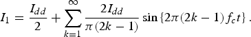 $$I_1 = \displaystyle{I_{dd} \over 2} + \sum_{k = 1}^{\infty} \displaystyle{2I_{dd} \over \pi \lpar 2k - 1\rpar } \sin \left\{2\pi \lpar 2k - 1\rpar f_c t \right\}.$$
From Fig. 1, the load impedance from switches Q1 and Q2 at frequency f, including parasitic resistance of the resonator, can be expressed as
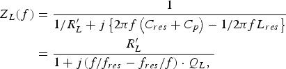 $$\eqalign{Z_L \lpar f\rpar & =\displaystyle{1 \over 1 / R^{\prime}_L + j \left\{2\pi f\left(C_{res} + C_p \right)- 1 / 2\pi fL_{res} \right\}} \cr & = \displaystyle{R^{\prime}_L \over 1 + j\lpar f / f_{res} - f_{res} / f\rpar \cdot Q_L\comma \; }}$$
where R′ L = (1 − Q L/Q u) R L. From equation (A1), the current through the load impedance is calculated as
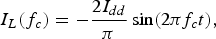
 $$I_L = I_{dd} - I_1 = - \sum_{k = 1}^{\infty} \displaystyle{2I_{dd} \over \pi \lpar 2k - 1\rpar } \sin \left\{2\pi \lpar 2k - 1\rpar f_c t \right\}.$$
From equations (A2) and (A3), the voltage shown at the load impedance is calculated as
 $$\eqalign{& V_L =Z_L \lpar f\rpar \circ I_L \cr &= - \displaystyle{2R^{\prime}_L I_{dd} \over \pi} \sum_{k = 1}^{\infty} \displaystyle{\sin \left\{2\pi \lpar 2k - 1\rpar f_c t \right\}- n\lpar k\rpar Q_L \cos \left\{2\pi \lpar 2k - 1\rpar f_c t \right\}\over \lpar 2k - 1\rpar \left\{1 + n\lpar k\rpar ^2 Q_L^2 \right\}\comma \; }}$$
where ○ is Volterra operator. From equations (A3) and (A4), the load current and voltage at the fundamental frequency are written as
 $$I_L \lpar f_c \rpar =- \displaystyle{2I_{dd} \over \pi} \sin \lpar 2\pi f_c t\rpar \comma \; $$
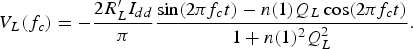 $$V_L \lpar f_c \rpar = - \displaystyle{2R^{\prime}_L I_{dd} \over \pi} \displaystyle{\sin \lpar 2\pi f_c t\rpar - n\lpar 1\rpar Q_L \cos \lpar 2\pi f_c t\rpar \over 1 + n\lpar 1\rpar ^2 Q_L^2}.$$
From equations (A5) and (A6), the output power delivered to R L is calculated as
 $$\eqalign{P_{out} &= \left(1 - \displaystyle{Q_L \over Q_u} \right)f_c \vint_0^{1 /f_c} I_L \lpar f_c \rpar V_L \lpar f_c \rpar dt \cr &= \displaystyle{2R^{\prime}_L I_{dd}^2 \over \pi^2} \left(1 - \displaystyle{Q_L \over Q_u} \right)\displaystyle{1 \over 1 + n\lpar 1\rpar ^2 Q_L^2}.} $$
From Fig. 1 and equation (A4), the DC component of V 1 is calculated as
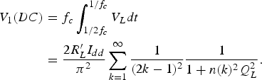 $$\eqalign{V_1 \lpar DC\rpar &= f_c \vint_{1 /2f_c}^{1 /f_c} V_L dt \cr &= \displaystyle{2R^{\prime}_L I_{dd} \over \pi ^2} \sum_{k = 1}^{\infty} \displaystyle{1 \over \lpar 2k - 1\rpar ^2} \displaystyle{1 \over 1 + n\lpar k\rpar ^2 Q_L^2}.}$$
From equation (A8), DC power consumption is calculated as
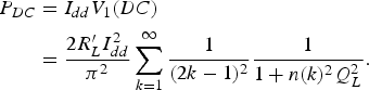 $$\eqalign{P_{DC} &= I_{dd} V_1 \lpar DC\rpar \cr &= \displaystyle{2R^{\prime}_L I_{dd}^2 \over \pi^2} \sum_{k = 1}^{\infty} \displaystyle{1 \over \lpar 2k - 1\rpar ^2} \displaystyle{1 \over 1 + n\lpar k\rpar ^2 Q_L^2}.}$$
From equations (A7) and (A9), the drain efficiency (η = P out/P DC) in equation (2) can be obtained.
When R on cannot be neglected, DC power consumption is expressed as
 $$P_{DC} = \displaystyle{2R^{\prime}_L I_{dd}^2 \over \pi^2} \sum_{k = 1}^{\infty} \displaystyle{1 \over \lpar 2k - 1\rpar ^2} \displaystyle{1 \over 1 + n\lpar k\rpar ^2 Q_L^2} + R_{on} I_{dd}^2.$$
From equations (A7) and (A10), drain efficiency in equation (3) is derived.
In addition, when C p also needs to be taken into account, the load voltage and current at the fundamental frequency are written as
 $$V_L \lpar f_c \rpar = - \displaystyle{2R^{\prime}_L I_{dd} \over \pi} \displaystyle{\sin \!\lpar 2\pi f_c t\rpar - n\lpar 1\rpar Q_L \cos\! \lpar 2\pi f_c t\rpar \over 1 + n\lpar 1\rpar ^2 Q_L^2} - \displaystyle{4\Delta V \over \pi} \sin \!\lpar 2\pi f_c t\rpar \comma \; $$
 $$I_L \lpar f_c \rpar =- \displaystyle{2I_{dd} \over \pi} \sin \!\lpar 2\pi f_c t\rpar - \displaystyle{4\Delta V \over \pi R^{\prime}_L} \left\{\sin \!\lpar 2\pi f_c t\rpar + n\lpar 1\rpar Q_L \cos \!\lpar 2\pi f_c t\rpar \right\}.$$
From equations (A11) and (A12), the output power in equation (5) is calculated. DC power consumption is expressed as
 $$P_{DC} = \displaystyle{2R^{\prime}_L I_{dd}^2 \over \pi ^2} \sum_{k = 1}^{\infty} \displaystyle{1 \over \lpar 2k - 1\rpar ^2} \displaystyle{1 \over 1 + n\lpar k\rpar ^2 Q_L^2} + R_{on} I_{dd}^2 + \Delta V I_{dd}$$
From equations (3) and (A13), drain efficiency in equation (6) is derived.
 Toshifumi Nakatani (M’01) received the B.E. and M.E. degrees in Electrical Engineering from Kyoto University, Japan, in 1994 and 1996, respectively, and is currently pursuing a Ph.D. degree from the University of California at San Diego (UCSD), La Jolla. In 1996, he joined the Matsushita Electric Industrial Co. Ltd. (now Panasonic Corporation), Osaka, Japan, where he was mainly involved with the modeling of RF silicon devices and the development of low noise amplifier and mixer for cell phone handset using SiGe BiCMOS technology. In 2008, he was with UCSD as a visiting scholar, and in 2010, he was with Panasonic Corporation of North America, Cupertino. In both places, he was involved in the development of digital assisted power amplifier for handset applications. In 2011, he joined WiGig 60 GHz IC project with Panasonic Corporation in Japan. His research interests include RF and analog IC design for wireless communication systems.
 Donald F. Kimball (S’82-M’83) was born in Cleveland, Ohio in 1959. He received the B.S.E.E. (Suma Cum Laude) with distinction and the M.S.E.E. at Ohio State University, Columbus, Ohio, in 1982 and 1983 respectively. From 1983 to 1986, he worked for Data General Corp. as a TEMPEST engineer. From 1986 to 1994, he worked at Data Products New England as an electromagnetic compatibility engineer/manager. From 1994 to 1999, he worked at Qualcomm, Inc. as a regulatory product approval engineer/manager. From 1999 to 2002, he worked at Ericsson, Inc. as a research & technology engineer/manager. Since 2003, he has been working at Calit2 at the University of California San Diego as a principal development engineer. He holds 7 U.S. patents associated with high power RF amplifiers (HPA). He has also published numerous technical papers high efficiency high linearity HPAs. His research interests include HPA envelope elimination and restoration techniques, switching HPAs, adaptive digital pre-distortion, memory effect inversion, mobile and portable wireless device battery management, and small electric powered radio controlled autonomous aircraft.
 Lawrence E. Larson received the BS in Electrical Engineering from Cornell University, Ithaca, and a PhD from UCLA. From 1980 to 1996, he was at Hughes Research Laboratories in Malibu, CA, where he directed the development of high-frequency microelectronics in GaAs, InP, and Si/SiGe and MEMS technologies. He joined the faculty at the University of California – San Diego, in 1996, where he was the inaugural holder of the Communications Industry Chair. He was the Director of the UCSD Center for Wireless Communications from 2001–2006 and was Chair of the Department of Electrical and Computer Engineering from 2007–2011. He moved to Brown University in 2011, where he is Dean of the School of Engineering. During the 2000–2001 academic year, he was on leave at IBM Research in San Diego, CA. During the 2004–2005 academic year, he was a visiting Professor at TU Delft, Netherlands. He was the recipient of the Hughes Sector Patent Award in 1994 for his work on RF MEMS, co-recipient of the 1996 Lawrence A. Hyland Patent Award of Hughes Electronics, for his work on low-noise millimeterwave HEMTs, and co-recipient of the 1999 IBM Microelectronics Excellence Award for his work in Si/SiGe HBT technology. He has published over 300 papers, received 40 US patents, co-authored three books, and is a Fellow of the IEEE.
 Peter M. Asbeck (M’75-SM’97-F’00) attended MIT, where he received the B.S. and Ph.D. degrees in 1969 and in 1975. He worked at the Sarnoff Research Center, Princeton, New Jersey, and at Philips Laboratory, Briarcliff Manor, New York, in the areas of quantum electronics and GaAlAs/GaAs laser physics. In 1978, he joined Rockwell International Science Center, where he was involved in the development of high speed devices and circuits using III–V compounds and heterojunctions. He pioneered efforts to develop heterojunction bipolar transistors based on GaAlAs/GaAs and InAlAs/InGaAs materials. In 1991, Dr Asbeck joined the University of California at San Diego, where he is the Skyworks Chair Professor in the Department of Electrical and Computer Engineering. His research interests are in development of high performance transistor technologies and their circuit applications. Dr Asbeck's research has led to more than 350 publications. He is a member of the National Academy of Engineering, and has been a Distinguished Lecturer of the IEEE Electron Device Society and of the Microwave Theory and Techniques Society. He received the 2003 IEEE David Sarnoff Award for his work on heterojunction bipolar transistors.


